
User's Manual
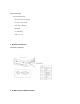
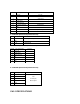
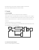
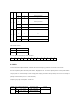
Table 3.1: Control power and frequency
Operation for transmit Mode is oscillated by Q21, C84, C85, C86, C87, C88, C89, C90, C91, VC12, D15, D16 and L26
They are consist of Colpitts Oscillator.).
R7 and C86 are circuit to remain 450 ~ 470 MHz frequency stable.
Varicap Diode determines frequency range for D15. D16 alters Data.
Operation for Receive Mode is oscillated by Q20, C73, C74, C75, C76, C77, C78, C79, D14 and L21.
Q22 and extra parts are buffers to amplify RF carrier which is oscillated by TX VCO and RX VCO, remain final output
0dB
m
±2dB and prevent amplified reverse power from output part.
2.3 Input Data ALC (Automatic Level Control)
User can use different input signal level.
Input Data ALC (Automatic Level Control) is designed to use every digital signal whose input signal range is 05V~0.6V.
Input signal data provided by D-sub Connector No. 4 pin amplify 47times as U16A and is provided to U16B Limiting
circuit. Output of U16B restricts every signal as 1.4V and provides to VCO and TCXO. TCXO (U17) alters data signal
(0~350Hz) with R63 and C64 and does not alter more than 350Hz with VCO. R60 is used as bypass, not using input
Data ALC(Automatic Level Control)circuit.
2.4 POWER DRIVE
TX Drive (Q24, Q25) amplify RF power occurring VCO to meet final AMP input and restrict influence of reverse power.
First amp (Q24) operate as A level and amplify VCO output about 15dB. Second amp(Q25) amplify about 10dB to
amplify final AMP(Q26) about 5W and to remain final output of C107 24~25dB. When P2.6 Port of MPU (U13) is high,
Q24 and Q25 turn Q31 on and TR(Q30) provide power to TX drive.
This power provides power to ANT S/W and turn on D10 and D11 to emit TX carrier through antenna.
2.5 Final AMP and APC