
User Manual

802.11g Wireless LAN+BT SiP combo Module V2.2
All rights are reserved by USI. No part of this technical document can be reproduced in any form without permission of USI
.
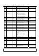
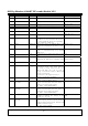
27
50 D15 HD15 CompactFlash Data bit[15] IO, PU, 4mA
51 D14 HD14 CompactFlash Data bit[14] IO, PU, 4mA
52 D13 HD13 CompactFlash Data bit[13] IO, PU, 4mA
53 D12 HD12 CompactFlash Data bit[12] IO, PU, 4mA
54 D11 HD11 CompactFlash Data bit[11] IO, PU, 4mA
55 N/A BT_LED_B BT LED control signal which drives the
LED to indicate the activity of Bluetooth.
Active low.
Output, 4mA
56 N/A RXD_B
UART Data input, active High, Pulled
down (weak)
Input, WPD, 1µA
57 N/A CTS_B UART Clear to Send, Active low, Pulled
down (weak)
Input, WPD, 1µA
58 N/A
SD_DAT0
PCM_CLK
Synchronous Data clock
SD_DAT0 : SDIO DATA LINE 0
59 N/A VCC_BT 3.3V supply voltage for Bluetooth
Input
60 GND
GND
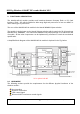
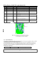
Fig 1: Pin 1 assignment and indication Drawing
( To be updated with latest design)
9.2.1. LED INTERFACE
The Wireless Module will provide two control signals to the host and capable to drive an LED
to indicate the connectivity and operating status.
The WM-BG-MR-01 have 2 LED’s (output) via 60 pins connector for feedback to the user on
the current WLAN activity state. The signaling will reflect status / activity as described in the
table below. Those two signals are provided via the board to board connector with the
following pin assignment.
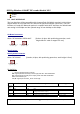
Pin No Pin description Function description
Pin 59
Pin 60
Pin 59
Pin 1
Pin 60