
User Manual

802.11g Wireless LAN+BT SiP combo Module V2.2
All rights are reserved by USI. No part of this technical document can be reproduced in any form without permission of USI
.
26
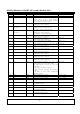
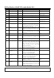
30 GND GND
31 GND GND
32 D10 HD10 CompactFlash Data bit[10]
IO, PU, 4mA
33 D09 HD9 CompactFlash Data bit[9] IO, PU, 4mA
34 D08 HD8 CompactFlash Data bit[8] IO, PU, 4mA
35 -STSCHG HSTSCHG
_B
Card status changed Output, 4mA
36 -SPKR PCM_Sync Synchronous Data strobe
Input PD, 4mA
37 -REG HREG_B Register select and I/O enable Input, PU
38 -INPACK HINPACK_
B
INPUT ACKNOWLEDGE is driven by WM-
BG-MR-01. Is asserted when the device
is selected and the device is responding
to an I/O Read command.
Output, 2mA
39 -WAIT HWAIT_B HWAIT_B is driven by WM-BG-MR-01 and
allows for extending the memory or I/O
cycle
Output, 4mA
40 RESET
HRESET
Used to asynchronously reset WLAN.
High active.
Input, PU
41 N/A N/A Reserved. Keep connection open on Host
side
N/A
42 N/A WLAN_LED
_B
WLAN LED control si
g
nal, driven the LED
indicating the link status of WLAN. Active
low.
Output, 4mA
43 N/A PCM_OUT Synchronous Data output
44 IREQ
IREQ_B Ready/Busy or Interrupt request.
In memory mode, this si
g
nal indicates
the ready or busy status of the card.
When held hi
g
h, the card is ready to
accept a new data transfer. When held
low the card is busy.
In I/O mode, this signal is used to
indicate an interrupt condition.
Output, 4mA
45 -WE HWE_B WRITE ENABLE is driven by the host
during a memory Write Access
Input, PU
46 -IOWR
SD_DAT3
HIOWR_B I/O Write Strobe is driven by the host
and is asserted when the host wants to
write to an on-chip I/O register
SD_DAT3 : SDIO DATA LINE 3
Input, PU
47 -IORD
SD_DAT1
HIORD_B I/O Read Strobe is driven by the host
and is asserted when the host wants to
read from an on-chip I/O register
SD_DAT1 : SDIO DATA LINE 1
Input, PU
48 -VS1 -VS1
T
his pin is connected to Ground on
module to indicate the volta
g
e of this
module is 3.3V card.
GND
49 -CE2
SD_CLK
HCE2_B CARD ENABLE2 is driven by the host
system and is used as select strobe in
both I/O and memory mode. Enables odd
numbered address bytes
SD_CLK : SDIO CLOCK
Input, PU