
Integration Instructions


P1D Broadband Module Integration
21 March 2001 Proprietary Information Page 3 of 11
Contents
1 General............................................................................................................................................ 5
1.1 Approvals and Dates ............................................................................................................... 5
1.2 Change Record ....................................................................................................................... 5
1.3 Acronyms ................................................................................................................................ 6
1.4 External References ................................................................................................................ 6
2 Introduction ..................................................................................................................................... 7
2.1 Scope of Document ................................................................................................................. 7
2.2 Overview of Module ................................................................................................................ 7
3 Module Connections ....................................................................................................................... 8
3.1 Data Interface J2 ..................................................................................................................... 8
3.1.1 Universal Serial Bus ........................................................................................................ 8
3.1.2 Ethernet ........................................................................................................................... 8
3.2 J2 Connector ........................................................................................................................... 8
3.2.1 Connector Type ............................................................................................................... 8
3.2.2 Pin Out ............................................................................................................................ 8
3.3 DC Power Input J1 .................................................................................................................. 9
3.4 Battery Contact J3 ................................................................................................................... 9
3.5 SIM Holder Socket 2 ............................................................................................................... 9
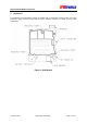
4 Mechanical .................................................................................................................................... 10
5 Regulatory Information .................................................................................................................. 11
5.1 Compliance with FCC Rules and Regulations ...................................................................... 11
5.2 Exposure to Radio Frequency Signals .................................................................................. 11
Figures
Figure 1: P1D Module ........................................................................................................................... 10
Tables
Table 1: 18 way Data Connector ............................................................................................................ 9