User's Manual
Table Of Contents
- Document history
- Introduction
- Product concept
- Application Interface
- Antenna interface
- Electrical, reliability and radio characteristics
- Mechanics
- Reference Approval
- Design example
- List of parts and accessories

MC55/56 Hardware Interface Description
Confidential / Preliminary
s
MC55/56_hd_v03.00 Page 66 of 104 16.08.2005
4 Antenna interface
The RF interface has an impedance of 50. MC55/56 is capable of sustaining a total
mismatch at the antenna connector or pad without any damage, even when transmitting at
maximum RF power.
The external antenna must be matched properly to achieve best performance regarding
radiated power, DC-power consumption and harmonic suppression. Matching networks are
not included on the MC55/56 PCB and should be placed in the host application.
Regarding the return loss MC55/56 provides the following values:
Table 20: Return loss
State of module Return loss of module Recommended return loss of application
Receive > 8dB > 12dB
Transmit not applicable > 12dB
Idle < 5dB not applicable
The connection of the antenna or other equipment must be decoupled from DC voltage.
4.1 Antenna installation
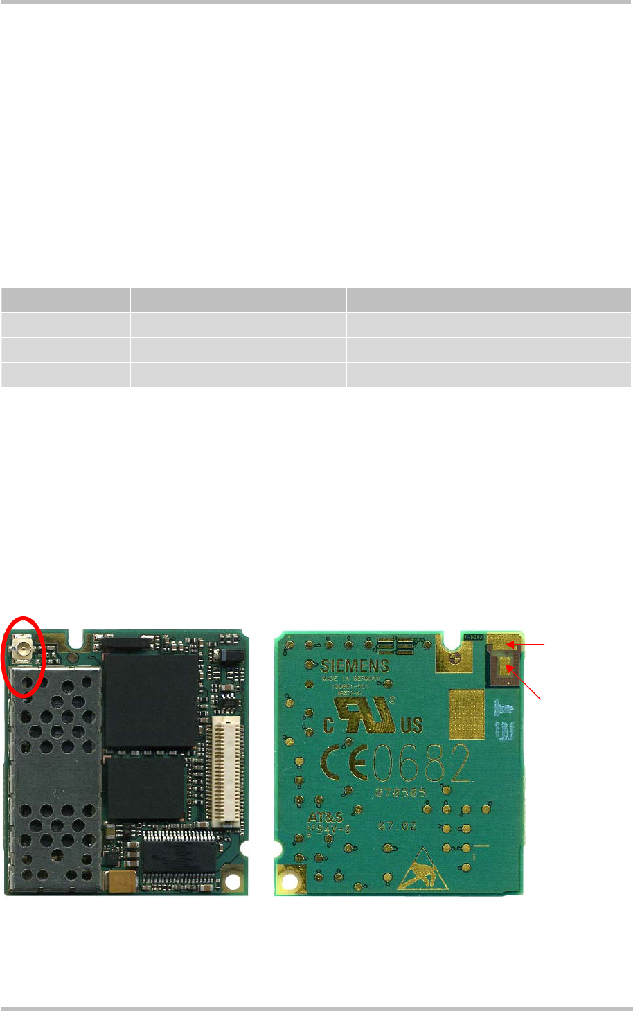
To suit the physical design of individual applications MC55/56 offers two alternative
approaches to connecting the antenna:
• Recommended approach: U.FL-R-SMT antenna connector from Hirose assembled on
the component side of the PCB (top view on MC55/56). See Chapter 4.1.2 for details.
• Antenna pad and grounding plane placed on the bottom side. See Chapter 4.1.1.
Figure 26: U.FL-R-SMT connector Figure 27: Antenna pad and GND plane
Antenna pad
Antenna ground


