User's Manual
Table Of Contents
- Document history
- Introduction
- Product concept
- Application Interface
- Antenna interface
- Electrical, reliability and radio characteristics
- Mechanics
- Reference Approval
- Design example
- List of parts and accessories

MC55/56 Hardware Interface Description
Confidential / Preliminary
s
MC55/56_hd_v03.00 Page 60 of 104 16.08.2005
3.11.2 Design considerations for SIM card holder
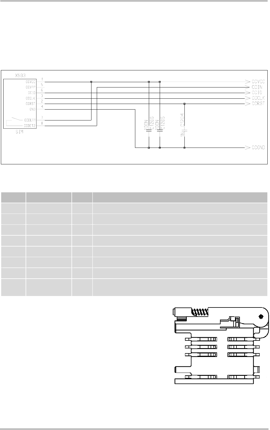
The schematic below is a sample configuration that illustrates the Molex SIM card holder
located on the DSB45 Support Box (evaluation kit used for type approval of the Siemens
MC55/56 reference setup, see [5]). X503 is the designation used for the SIM card holder in
[5].
Molex card holder
GSM module
Figure 20: SIM card holder of DSB45 Support Box
Table 16: Pin assignment of Molex SIM card holder on DSB45 Support Box
Pin no. Signal name I/O Function
1 CCVCC I Supply voltage for SIM card, generated by the GSM engine
2 CCRST I Chip card reset, prompted by the GSM engine
3 CCCLK I Chip card clock
4 CCGND - Individual ground line for the SIM card to improve EMC
5 CCVPP - Not connected
6 CCIO I/O Serial data line, bi-directional
7 CCDET1 - Connect to CCVCC
8 CCDET2 Connects to the CCIN input of the GSM engine. Serves to
recognize whether a SIM card is in the holder.
Pins 1 through 8 (except for 5) are the minimum
requirement according to the GSM Recommendations,
where pins 7 and 8 are needed for SIM card tray
detection through the CCIN pin.
Figure 21: Pin numbers of Molex SIM card holder on DSB45
Support Box
Place the capacitors C1205 and C1206 (or instead one capacitor of 200nF) as close as
possible to the pins 1 (CCVCC) and 4 (GND) of the card holder. Connect the capacitors to
the pins via low resistance tracks.
4
5
1
2
7
8
3
6


