User's Manual
Table Of Contents
- Document history
- Introduction
- Product concept
- Application Interface
- Antenna interface
- Electrical, reliability and radio characteristics
- Mechanics
- Reference Approval
- Design example
- List of parts and accessories

MC55/56 Hardware Interface Description
Confidential / Preliminary
s
MC55/56_hd_v03.00 Page 21 of 104 16.08.2005
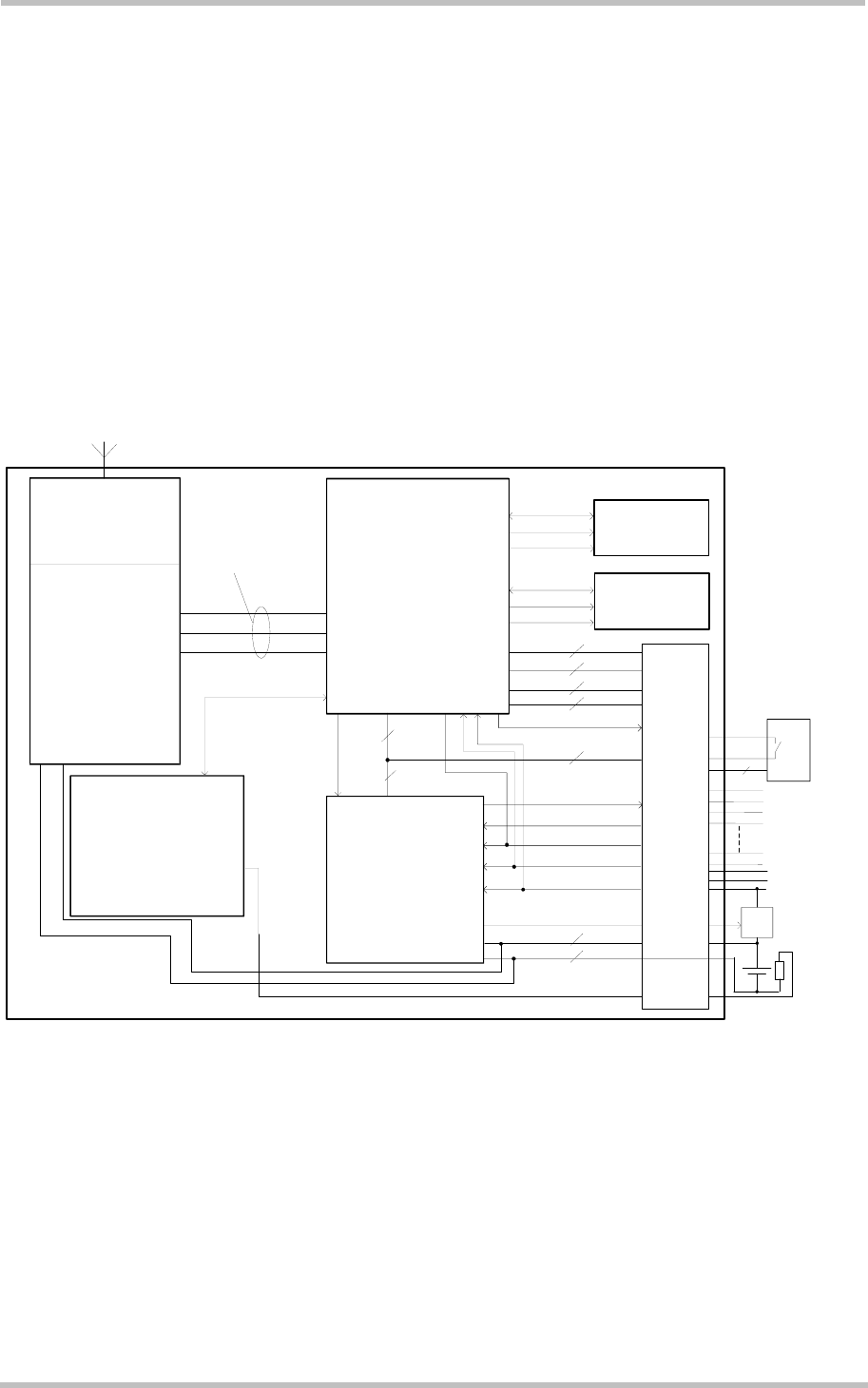
2.2 Circuit concept
Figure 1 shows a block diagram of the MC55/56 module and illustrates the major functional
components:
GSM / GPRS baseband block:
• Baseband controller operating at 26MHz
• Power supply ASIC
• Stacked Flash / SRAM
• Application interface (board-to-board connector)
GSM RF block:
• Skyworks RF transceiver
• Skyworks RF power amplifier / FEM
• RF front end (antenna connector)
Baseband
Controller
Power
Supply
ASIC
SIM
BATT+
GND
/IGT
/EMERGOFF
ASC1
ASC0
4
2x Audio
SIM Interface
CCRST
CCCLK
CCIO
CCIN
Receive
Send
Control
MC5x
Interface
RF - Baseband
5
5
Measuring
Network
4
CCIN
CCVCC
POWER
BATT_TEMP
VDDLP
SYNC
VDD
RF Section
RF Power
Amplifier
Data
Adr
Control
SRAM
Flash
CHARGE
6
8
9
DAI
5
4
Charger
input
+
Ext.
Charging
Circuit
NTC
Application Interface
(50 pins)
CCVCC
(GND)
2
Data
Adr
Control
Figure 1: MC55/56 block diagram


