
User's Manual

AC65/AC75 Hardware Interface Description
Confidential / Preliminary
s
AC65/AC75_hd_v00.372 Page 70 of 118 2006-08-03
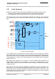
Table 16 shows the assignment of the DAI0…6 pins to the PCM interface signals. To avoid
hardware conflicts different pins are used as inputs and outputs for frame sync and clock
signals in master or slave operation. The table shows also which pin is used for master or
slave. The data pins (TXDAI and RXDAI) however are used in both modes. Unused inputs
have to be tied to GND, unused outputs must be left open.
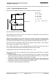
Table 16: Overview of DAI pin functions
Signal name on
B2B connector
Function for PCM Interface Input/Output
DAI0 TXDAI Master/Slave O
DAI1 RXDAI Master/Slave I
DAI2 FS (Frame sync) Master O
DAI3 BITCLK Master O
DAI4 FSIN Slave I
DAI5 BCLKIN Slave I
DAI6 nc I
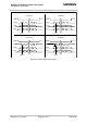
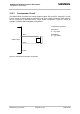
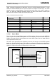
3.15.4.1 Master Mode
To clock input and output PCM samples the PCM interface delivers a bit clock (BITCLK)
which is synchronous to the GSM system clock. The frequency of the bit clock is 256kHz or
512kHz. Any edge of this clock deviates less than ±100ns (Jitter) from an ideal 256-kHz
clock respective 512-kHz-clock.
The frame sync signal (FS) has a frequency of 8 kHz and is high for one BITCLK period
before the data transmission starts if short frame is configured. If long frame is selected the
frame sync signal (FS) is high during the whole transfer of the 16 data bits. Each frame has a
duration of 125µs and contains 32 respectively 64 clock cycles.
BITCLK
FS
TXDAI
RXDAI
bitclk
frame sync
TX_data
RX_data
Codec
PCM interface of
the GSM module
Figure 28: Master PCM interface Application