
User's Manual

AC65/AC75 Hardware Interface Description
Confidential / Preliminary
s
AC65/AC75_hd_v00.372 Page 22 of 118 2006-08-03
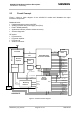
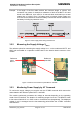
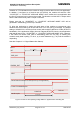
2.3 Circuit Concept
Figure 1 shows a block diagram of the AC65/AC75 module and illustrates the major
functional components:
Baseband block:
• Digital baseband processor with DSP
• Analog processor with power supply unit (PSU)
• Flash / SRAM (stacked)
• Application interface (board-to-board connector)
• Antenna diagnostic
RF section:
• RF transceiver
• RF power amplifier
• RF front end
• Antenna connector
Digital Baseband
Processer with DSP
BATT+
GND
IGT
EMERG_RST
ASC(0)
5
SIM Interface
CCIN
CCRST
CCIO
CCCLK
CCVCC
D(0:15)
A(0:24)
RD; WR; CS; WAIT
RF Control Bus
Interface
RF - Baseband
NTC
BATT_TEMP
VDDLP
SYNC
Transceiver
RF Power
Amplifier
SRAM
Flash
6
5
8
8
AC65/AC75
I / Q
4
Audio analog
DAC_OUT
10
USB
GPIO
3
10
I2C/SPI
SPI
2
2
VEXT
ISENSE
VSENSE
VCHARGE
CHARGEGATE
3
RESET
BATTYPE
TEMP2
REFCHG
ASC(1)
4
26MHz
Front End
DAI
7
PWR_IND
Measuring
Network
32.768kHz
26MHz
RTC
Application Interface (80 pin)
RF-Part
Analog
Controller
with PSU
Reset
Antenna
Diagnostic
ADC
Figure 2: AC65/AC75 block diagram