
Manual

GE
Data Sheet
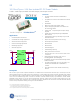
12V MicroTLynx
TM
12A: Non-Isolated DC-DC Power Modules
4.5Vdc –14Vdc input; 0.69Vdc to 5.5Vdc output; 12A Output Current
May 2, 2013 ©2013 General Electric Company. All rights reserved. Page 5
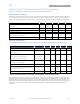
Feature Specifications
Unless otherwise indicated, specifications apply over all operating input voltage, resistive load, and temperature conditions. See
Feature Descriptions for additional information.
Parameter Device Symbol Min Typ Max Unit
On/Off Signal Interface
(V
IN
=V
IN, min
to V
IN, max
; open collector or equivalent,
Signal referenced to GND)
Device is with suffix “4” – Positive Logic (See Ordering Information)
Logic High (Module ON)
Input High Current All IIH
—
⎯
25 µA
Input High Voltage All VIH
V
IN
– 1
⎯
V
IN,max
V
Logic Low (Module OFF)
Input Low Current All IIL
⎯ ⎯
3 mA
Input Low Voltage All VIL
⎯ ⎯
3.5 V
Device Code with no suffix – Negative Logic (See Ordering
Information)
(On/OFF pin is open collector/drain logic input with
external pull-up resistor; signal referenced to GND)
Logic High (Module OFF)
Input High Current All IIH — — 1 mA
Input High Voltage All VIH 2.0 — V
IN, max
Vdc
Logic Low (Module ON)
Input low Current All IIL — — 10 μA
Input Low Voltage All VIL 0 — 1 Vdc
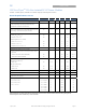
Turn-On Delay and Rise Times
(V
IN
=V
IN, nom
, I
O
=I
O, max ,
V
O
to within ±1% of steady state)
Case 1: On/Off input is enabled and then input power is
applied (delay from instant at which V
IN
= V
IN, min
until Vo =
10% of V
o, set)
All Tdelay — 2 — msec
Case 2: Input power is applied for at least one second and
then the On/Off input is enabled (delay from instant at
which Von/Off is enabled until V
o = 10% of Vo, set)
All Tdelay — 2 — msec
Output voltage Rise time (time for Vo to rise from
10% of Vo, set to 90% of Vo, set)
All Trise
— 5 — msec
Output voltage overshoot (T
A
= 25
o
C 3.0 % V
O, set
V
IN
= V
IN, min
to V
IN, max
,I
O
= I
O, min
to I
O, max
)
With or without maximum external capacitance
Over Temperature Protection All T
ref
133 °C
(See Thermal Considerations section)
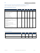
Sequencing Delay time
Delay from V
IN, min
to application of voltage on SEQ pin All TsEQ-delay 10 msec
Tracking Accuracy (Power-Up: 0.5V/ms) All VSEQ –Vo 100 mV
(Power-Down: 0.5V/ms) All VSEQ –Vo 150 mV
(V
IN, min
to V
IN, max
; I
O, min
to I
O, max
VSEQ
< Vo)
Input Undervoltage Lockout
Turn-on Threshold All
4.45 Vdc
Turn-off Threshold All
4.2 Vdc
Hysteresis All
0.25 Vdc