
Service Manual

CIRCUIT DESCRIPTION
4-7
Part No. 001-3474-002
When J201, pin 4 is high in receive, Q834 is turned off, Q101 is turned on and the collector voltage goes low.
A low on the base of Q102 turns the transistor on and the regulated +5.5V on the emitter is on the collector for the
receive circuitry. With a low on the base of Q831 the transistor is off and the collector is high. With a high on the
collector of Q831 and a low on the emitter of Q834, this reverse biases CR850 for a high impedance.
The capacitive leg is formed by C851, CR850, C852 and C876. When J201, pin 4 is low in transmit, Q834 is
turned on and a high is on the emitter, Q101 is turned off and the collector voltage goes high. A high on the base of
Q102 turns the transistor off and the regulated +5.5V is removed from the receive circuitry. With a high on the
base of Q831 the transistor is on and the collector is low. With a low on the collector of Q831 and a high on the
emitter of Q834, this forward biases CR850 and provides an RF ground through C851 and C852/C876 are
effectively connected to the tank circuit. This decreases the resonant frequency of the tank circuit.
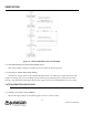
4.2.8 SYNTHESIZER INTEGRATED CIRCUIT (U801)
Introduction
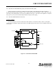
Synthesizer chip U801 is shown in Figure 4-2. This device contains the following circuits: R (reference),
Fractional-N, NM1 and NM2; phase and lock detectors, prescaler and counter programming circuitry. The basic
operation was described in Section 4.2.1.
Channel Programming
Frequencies are selected by programming the R, Fractional-N, NM1 and NM2 in U801 to divide by a certain
number. These counters are programmed by a user supplied programming circuit. More information on
programming is located in Section .
As previously stated, the counter divide numbers are chosen so that when the VCO is oscillating on the
correct frequency, the VCO-derived input to the phase detector is the same frequency as the reference oscillator-
derived frequency.
The VCO frequency is divided by the internal prescaler and the main divider to produce the input to the phase
detector.
4.2.9 LOCK DETECT
When the synthesizer is locked on frequency, the SYNTH LOCK output of U801, pin 18 (J201, pin 7) is a
high voltage. Then when the synthesizer is unlocked, the output is a low voltage. Lock is defined as a phase
difference of less than 1 cycle of the TCXO.