C141-E042-01EN MHA2021AT, MHA2032AT DISK DRIVES PRODUCT MANUAL
FOR SAFE OPERATION Handling of This Manual This manual contains important information for using this product. Read thoroughly before using the product. Use this product only after thoroughly reading and understanding especially the section “Important Alert Items” in this manual. Keep this manual handy, and keep it carefully. FUJITSU makes every effort to prevent users and bystanders from being injured or from suffering damage to their property. Use the product according to this manual.
Revision History (1/1) Edition Date Revised section (*1) (Added/Deleted/Altered) Details 01 1997-07-15 — — *1 Section(s) with asterisk (*) refer to the previous edition when those were deleted.
Preface This manual describes the MHA2021AT and MHA2032AT, 2.5-inch hard disk drives. These drives have a built-in controller that is compatible with the ATA interface. This manual describes the specifications and functions of the drives and explains in detail how to incorporate the drives into user systems. This manual assumes that the reader has a basic knowledge of hard disk drives and their implementations in computer systems.
Preface Abbreviation This section gives the meanings of the definitions used in this manual. Conventions for Alert Messages This manual uses the following conventions to show the alert messages. An alert message consists of an alert signal and alert statements. The alert signal consists of an alert symbol and a signal word or just a signal word.
Preface To make this manual easier for users to understand, opinions from readers are needed. Please write your opinions or requests on the Comment at the back of this manual and forward it to the address described in the sheet. Liability Exception “Disk drive defects” refers to defects that involve adjustment, repair, or replacement.
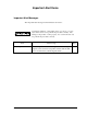
Important Alert Items Important Alert Messages The important alert messages in this manual are as follows: A hazardous situation could result in minor or moderate personal injury if the user does not perform the procedure correctly. Also, damage to the predate or other property, may occur if the user does not perform the procedure correctly. Task Normal Operation C141-E042-01EN Alert message Data corruption: Avoid mounting the disk near strong magnetic soures such as loud speakers.
Contents CHAPTER 1 Device Overview ....................................................................... 1-1 1.1 1.1.1 1.1.2 1.1.3 1.2 1.2.1 1.2.2 CHAPTER 2 1-2 Functions and performance Adaptability 1-2 Interface 1-2 Device Specifications 1-2 1-4 Specifications summary 1-4 Model and product number 1-5 1.3 Power Requirements 1.4 Environmental Specifications 1.5 Acoustic Noise 1.6 Shock and Vibration 1.7 Reliability 1-8 1.8 Error Rate 1-9 1.
Contents CHAPTER 3 Installation Conditions ..............................................................3-1 3.1 Dimensions 3.2 Mounting 3.3 Cable Connections 3.3.1 3.3.2 3.3.3 3.3.4 3.4 3.4.1 3.4.2 3.4.3 3.4.
Contents 4.6.3 4.6.4 4.7 4.7.1 4.7.2 4.7.3 4.7.4 4.7.5 CHAPTER 5 Servo Control 4-13 4-14 Servo control circuit 4-14 Data-surface servo format 4-18 Servo frame format 4-18 Actuator motor control 4-19 Spindle motor control 4-20 Interface ..................................................................................... 5-1 5.1 5.1.1 5.1.2 5.2 5.2.1 5.2.2 5.2.3 5.3 5.3.1 5.3.2 5.3.3 5.4 5.4.1 5.4.2 5.4.3 5.4.4 5.4.5 5.5 5.5.1 5.5.2 5.5.3 5.5.
Contents CHAPTER 6 Operations..................................................................................6-1 6.1 6.1.1 6.1.2 6.1.3 6.1.4 6.2 6.2.1 6.2.2 6.3 6.3.1 6.3.2 6.4 6.4.1 6.4.2 6.5 6.5.1 6.5.2 6.5.3 6.
Contents Illustrations Figures Figure 1.1 Current fluctuation (Typ.) at +5V when power is turned on Figure 2.1 Figure 2.2 Figure 2.3 Figure 2.4 Disk drive outerview 2-2 Configuration of disk media heads 1 drive system configuration 2-4 2 drives configuration 2-5 Figure 3.1 Figure 3.2 Figure 3.3 Figure 3.4 Figure 3.5 Figure 3.6 Figure 3.7 Figure 3.8 Figure 3.9 Figure 3.10 Figure 3.11 Figure 3.12 Figure 3.13 Figure 3.
Contents Figure 5.6 Figure 5.7 Figure 5.8 Figure 5.9 Figure 5.10 Figure 5.11 Protocol for the command execution without data transfer Normal DMA data transfer 5-75 Data transfer timing 5-77 Single word DMA data transfer timing (mode 2) 5-78 Multiword DMA data transfer timing (mode 2) 5-79 Power on Reset Timing 5-80 5-73 Figure 6.1 Figure 6.2 Figure 6.3 Figure 6.4 Figure 6.5 Figure 6.6 Figure 6.7 Figure 6.8 Figure 6.
Contents Table 5.10 Contents of security password 5-59 Table 5.11 Contents of SECURITY SET PASSWORD data 5-64 Table 5.12 Relationship between combination of Identifier and Security level, and operation of the lock function 5-65 Table 5.13 Command code and parameters 5-67 Table 6.
CHAPTER 1 Device Overview 1.1 Features 1.2 Device Specifications 1.3 Power Requirements 1.4 Environment Specifications 1.5 Acoustic Noise 1.6 Shock and Vibration 1.7 Reliability 1.8 Error Rate 1.9 Media Defects Overview and features are described in this chapter, and specifications and power requirement are described. The MHA2021AT and MHA2032AT are 2.5-inch hard disk drives with built-in disk controllers.
Device Overview 1.1 Features 1.1.1 Functions and performance (1) Compact The disk has 1 or 2 disks of 65 mm (2.5 inches) diameter, and its height is 12.5 mm (0.492 inch). (2) Large capacity The disk drive can record up to 1,083 MB (formatted) on one disk using the (8/9) PRML recording method and 13 recording zone technology. The MHA2021AT and MHA2032AT have a formatted capacity of 2,167 MB and 3,251 MB respectively. (3) High-speed Transfer rate The disk drive has an internal data rate up to 8.92 MB/s.
1.1 Features (2) 128-KB data buffer The disk drive uses a 128-KB data buffer to transfer data between the host and the disk media. In combination with the read-ahead cache system described in item (3) and the write cache described in item (7), the buffer contributes to efficient I/O processing. (3) Read-ahead cache system After the execution of a disk read command, the disk drive automatically reads the subsequent data block and writes it to the data buffer (read ahead operation).
Device Overview 1.2 Device Specifications 1.2.1 Specifications summary Table 1.1 shows the specfications of the disk drive. Table 1.1 Specifications Format Capacity (*1) Number of Heads MHA2021AT MHA2032AT 2.16 GB 3.25 GB 4 6 Number of Cylinders (User) 6,372 Bytes per Sector 512 Recording Method (8/9) PRML Track Density 10,555 TPI Bit Density 157,422 BPI Rotational Speed 4,000 rpm ± 1% Average Latency 7.
1.3 Power Requirements *1: Capacity under the LBA mode. Under the CHS mode (normal BIOS specification), formatted capacity, number of cylinders, number of heads, and number of sectors are as follows. Model Formatted Capacity No. of Cylinder No. of Heads No. of Sectors MHA2021AT 2,167.60 MB 4,200 16 63 MHA2032AT 3,251.40 MB 6,300 16 63 1.2.2 Model and product number Table 1.2 lists the model names and product numbers. Table 1.
Device Overview (3) Current Requirements and Power Dissipation Table 1.3 lists the current and power dissipation. Table 1.3 Current and power dissipation Typical RMS Current Typical Power (*2) 1.0 A Watts 5.0 W 0.236 A T.B.D T.B.D 1.18 W R/W (*3) 0.5 A T.B.D T.B.D 2.5 W Standby 0.076 A T.B.D T.B.D 0.38 W 0.03 AT.B.D T.B.D 0.15 W Spin up (*1) Idle Sleep *1 Current at starting spindle motor. *2 Power requirements reflect nominal values for +5V power. *3 At 30% disk accessing.
1.5 Acoustic Noise 1.4 Environmental Specifications Table 1.4 lists the environmental specifications. Table 1.
Device Overview 1.6 Shock and Vibration Table 1.6 lists the shock and vibration specification. Table 1.6 Shock and vibration specification Vibration (swept sine, one octave per minute) • Operating 5 to 500 Hz, 1.0G0-peak (without non-recovered errors) (9.
1.9 Media Defects (3) Service life In situations where management and handling are correct, the disk drive requires no overhaul for five years when the DE surface temperature is less than 48°C. When the DE surface temperature exceeds 48°C, the disk drives requires no overhaul for five years or 20,000 hours of operation, whichever occurs first. Refer to item (3) in Subsection 3.2 for the measurement point of the DE surface temperature.
CHAPTER 2 Device Configuration 2.1 Device Configuration 2.2 System Configuration This chapter describes the internal configurations of the hard disk drives and the configuration of the systems in which they operate.
Device Configuration 2.1 Device Configuration Figure 2.1 shows the disk drive. The disk drive consists of a disk enclosure (DE), read/write preamplifier, and controller PCA. The disk enclosure contains the disk media, heads, spindle motors, actuators, and a circulating air filter. Figure 2.1 Disk drive outerview (1) Disk The outer diameter of the disk is 65 mm. The inner diameter is 20 mm. The number of disks used varies with the model, as described below.
2.1 Device Configuration Head 0 Head 0 1 1 2 3 2 4 3 5 MHA2021AT MHA2032AT Figure 2.2 Configuration of disk media heads (3) Spindle motor The disks are rotated by a direct drive Hall-less DC motor. (4) Actuator The actuator uses a revolving voice coil motor (VCM) structure which consumes low power and generates very little heat. The head assembly at the edge of the actuator arm is controlled and positioned by feedback of the servo information read by the read/write head.
Device Configuration (5) Air circulation system The disk enclosure (DE) is sealed to prevent dust and dirt from entering. The disk enclosure features a closed loop air circulation system that relies on the blower effect of the rotating disk. This system continuously circulates the air through the circulation filter to maintain the cleanliness of the air within the disk enclosure. (6) Read/write circuit The read/write circuit uses a LSI chip for the read/write preamplifier.
2.2 System Configuration 2.2.3 2 drives connection (Host adaptor) MHA2021AT MHA2032AT MHA2021AT MHA2032AT Note: When the drive that is not conformed to ATA is connected to the disk drive above configuration, the operation is not guaranteed. Figure 2.4 2 drives configuration HA (host adaptor) consists of address decoder, driver, and receiver. ATA is an abbreviation of “AT attachment”. The disk drive is conformed to the ATA-3 interface.
CHAPTER 3 Installation Conditions 3.1 Dimensions 3.2 Mounting 3.3 Cable Connections 3.4 Jumper Settings This chapter gives the external dimensions, installation conditions, surface temperature conditions, cable connections, and switch settings of the hard disk drives.
Installation Conditions 3.1 Dimensions Figure 3.1 illustrates the dimensions of the disk drive and positions of the mounting screw holes. All dimensions are in mm. Figure 3.
3.2 Mounting 3.2 Mounting (1) Orientation Figure 3.2 illustrates the allowable orientations for the disk drive. (a) Horizontal –1 (b) Horizontal –1 (c) Vertical –1 (d) Vertical –2 (e) Vertical –3 (f) Vertical –4 Figure 3.
Installation Conditions (2) Frame The MR head bias of the HDD disk enclosure (DE) is zero. The mounting frame is connected to SG. Use M3 screw for the mounting screw and the screw length should satisfy the specification in Figure 3.3. The tightening torque must not exceed 3 kgcm. When attaching the HDD to the system frame, do not allow the system frame to touch parts (cover and base) other than parts to which the HDD is attached. (3) Limitation of side-mounting Do not use the center hole.
3.2 Mounting (4) Ambient temperature The temperature conditions for a disk drive mounted in a cabinet refer to the ambient temperature at a point 3 cm from the disk drive. The ambient temperature must satisfy the temperature conditions described in Section 1.4, and the airflow must be considered to prevent the DE surface temperature from exceeding 60°C. Provide air circulation in the cabinet such that the PCA side, in particular, receives sufficient cooling.
Installation Conditions (5) Service area Figure 3.5 shows how the drive must be accessed (service areas) during and after installation. Mounting screw hole Cable connection Mounting screw hole Figure 3.5 Service area (6) External magnetic fields Data corruption: Avoid mounting the disk drive near strong magnetic sources such as loud speakers. Ensure that the disk drive is not affected by external magnetic fields.
3.3 Cable Connections 3.3 Cable Connections 3.3.1 Device connector The disk drive has the connectors and terminals listed below for connecting external devices. Figure 3.6 shows the locations of these connectors and terminals. PCA Connector, setting pins Figure 3.
Installation Conditions 3.3.2 Cable connector specifications Table 3.2 lists the recommended specifications for the cable connectors. Table 3.2 Cable connector specifications ATA interface and power supply cable (44-pin type) Name Model Manufacturer Cable socket (44-pin type) 89361-144 BERG Cable (44-pin type) FV08-A440 Junkosha For the host interface cable, use a ribbon cable.
3.4 Jumper Settings 3.3.4 Power supply connector (CN1) Figure 3.8 shows the pin assignment of the power supply connector (CN1). Figure 3.8 Power supply connector pins (CN1) 3.4 Jumper Settings 3.4.1 Location of setting jumpers Figure 3.9 shows the location of the jumpers to select drive configuration and functions. Figure 3.
Installation Conditions 3.4.2 Factory default setting Figure 3.10 shows the default setting position at the factory. Figure 3.10 Factory default setting 3.4.3 Master drive-slave drive setting Master device (device #0) or slave device (device #1) is selected. Figure 3.11 Jumper setting of master or slave device Note: Pins A and C should be open.
3.4 Jumper Settings 3.4.4 CSEL setting Figure 3.12 shows the cable select (CSEL) setting. Note: The CSEL setting is not depended on setting between pins Band D. Figure 3.12 CSEL setting Figure 3.13 and 3.14 show examples of cable selection using unique interface cables. By connecting the CSEL of the master device to the CSEL Line (conducer) of the cable and connecting it to ground further, the CSEL is set to low level. The device is identified as a master device.
Installation Conditions Figure 3.
CHAPTER 4 Theory of Device Operation 4.1 Outline 4.2 Subassemblies 4.3 Circuit Configuration 4.4 Power-on sequence 4.5 Self-calibration 4.6 Read/Write circuit 4.7 Servo Control This chapter explains basic design concepts of the disk drive. Also, this chapter explains subassemblies of the disk drive, each sequence, servo control, and electrical circuit blocks.
Theory of Device Operation 4.1 Outline This chapter consists of two parts. First part (Section 4.2) explains mechanical assemblies of the disk drive. Second part (Sections 4.3 through 4.7) explains a servo information recorded in the disk drive and drive control method. 4.2 Subassemblies The disk drive consists of a disk enclosure (DE) and printed circuit assembly (PCA). The DE contains all movable parts in the disk drive, including the disk, spindle, actuator, read/write head, and air filter.
4.2 Subassemblies Head Head 0 0 1 1 2 3 2 4 3 5 MHA2021AT MHA2032AT Figure 4.1 Head structure 4.2.3 Spindle The spindle consists of a disk stack assembly and spindle motor. The disk stack assembly is activated by the direct drive sensor-less DC spindle motor, which has a speed of 4,000 rpm ±1%. The spindle is controlled with detecting a PHASE signal generated by counter electromotive voltage of the spindle motor at starting. 4.2.
Theory of Device Operation 4.3 Circuit Configuration Figure 4.2 shows the disk drive circuit configuration. (1) Read/write circuit The read/write circuit consists of two LSIs; read/write preamplifier (PreAMP) and read channel (RDC). The PreAMP consists of the write current switch circuit, that flows the write current to the head coil, and the voltage amplifier circuit, that amplitudes the read output from the head.
4.3 Circuit Configuration Figure 4.
Theory of Device Operation 4.4 Power-on Sequence Figure 4.3 describes the operation sequence of the disk drive at power-on. The outline is described below. a) After the power is turned on, the disk drive executes the MPU bus test, internal register read/write test, and work RAM read/write test. When the self-diagnosis terminates successfully, the disk drive starts the spindle motor. b) The disk drive executes self-diagnosis (data buffer read/write test) after enabling response to the ATA bus.
4.5 Self-calibration Figure 4.3 Power-on operation sequence 4.5 Self-calibration The disk drive occasionally performs self-calibration in order to sense and calibrate mechanical external forces on the actuator, and VCM tarque. This enables precise seek and read/write operations. 4.5.1 Self-calibration contents (1) Sensing and compensating for external forces The actuator suffers from torque due to the FPC forces and winds accompanying disk revolution.
Theory of Device Operation The forces are compensated by adding the measured value to the specified current value to the power amplifier. This makes the stable servo control. To compensate torque varing by the cylinder, the disk is divided into 8 areas from the innermost to the outermost circumference and the compensating value is measured at the measuring cylinder on each area at factory calibration. The measured values are stored in the SA cylinder.
4.6 Read/write Circuit Table 4.1 Self-calibration execution timechart Time elapsed Time elapsed (accumulated) 1 At power-on Initial calibration 2 About 5 minutes About 5 minutes 3 About 5 minutes About 10 minutes 4 About 10 minutes About 20 minutes 5 About 10 minutes About 30 minutes 6 About 15 minutes About 45 minutes 7 About 15 minutes About 60 minutes 8 . . . . Every about 30 minutes 4.5.
Theory of Device Operation signal (WUS) when a write error occurs due to head short-circuit or head disconnection. 4.6.2 Write circuit The write data is output from the hard disk controller (HDC) with the NRZ data format, and sent to the encoder circuit in the RDC with synchronizing with the write clock. The NRZ write data is converted from 8-bit data to 9-bit data by the encoder circuit then sent to the PreAMP, and the data is written onto the media.
4.6 Read/write Circuit Figure 4.
Theory of Device Operation 4.6.3 Read circuit The head read signal from the PreAMP is regulated by the automatic gain control (AGC) circuit. Then the output is converted into the sampled read data pulse by the programmable filter circuit and the adaptive equalizer circuit. This clock signal is converted into the NRZ data by the 8/9 GCR decoder circuit based on the read data maximum-likelihood-detected by the Viterbi detection circuit, then is sent to the HDC.
4.6 Read/write Circuit (4) Viterbi detection circuit The sample hold waveform output from the adaptive equalizer circuit is sent to the Viterbi detection circuit. The Viterbi detection circuit demodulates data according to the survivor path sequence. (5) Data separator circuit The data separator circuit generates clocks in synchronization with the output of the adaptive equalizer circuit. To write data, the VFO circuit generates clocks in synchronization with the clock signals from a synthesizer.
Theory of Device Operation 4.7 Servo Control The actuator motor and the spindle motor are submitted to servo control. The actuator motor is controlled for moving and positioning the head to the track containing the desired data. To turn the disk at a constant velocity, the actuator motor is controlled according to the servo data that is written on the data side beforehand. 4.7.1 Servo control circuit Figure 4.6 is the block diagram of the servo control circuit.
4.7 Servo Control The major internal operations are listed below. a. Spindle motor start Starts the spindle motor and accelerates it to normal speed when power is applied. b. Move head to reference cylinder Drives the VCM to position the head at the any cylinder in the data area. The logical initial cylinder is at the outermost circumference (cylinder 0). c. Seek to specified cylinder Drives the VCM to position the head to the specified cylinder. d.
Theory of Device Operation Figure 4.
4.7 Servo Control (2) Servo burst capture circuit The servo burst capture circuit reproduces signals (position signals) that indicate the head position from the servo data on the data surface. SERVO A, SERVO B, SERVO C and SERVO D burst signals shown in Figure 4.8 followed the servo mark, cylinder gray and index information are output from the servo area on the data surface via the data head.
Theory of Device Operation 4.7.2 Data-surface servo format Figure 4.7 describes the physical layout of the servo frame. The three areas indicated by (1) to (3) in Figure 4.7 are described below. (1) Inner guard band The head is in contact with the disk in this space when the spindle starts turning or stops, and the rotational speed of the spindle can be controlled on this cylinder area for head moving. (2) Data area This area is used as the user data area SA area.
4.7 Servo Control (1) Write/read recovery This area is used to absorb the write/read transient and to stabilize the AGC. (2) Servo mark This area gererates a timing for demodulating the gray code and positiondemodulating the servo A to D by detecting the servo mark. (3) Gray code (including index bit) This area is used as cylinder address.
Theory of Device Operation d) If the head is stopped at the reference cylinder from there. Track following control starts. (2) Seek operation Upon a data read/write request from the host, the MPU confirms the necessity of access to the disk. If a read/write instruction is issued, the MPU seeks the desired track. The MPU feeds the VCM current via the D/A converter and power amplifier to move the head.
4.7 Servo Control d) During phase switching, the spindle motor starts rotating in low speed, and generates a counter electromotive force. The SVC detects this counter electromotive force and reports to the MPU using a PHASE signal for speed detection. e) The MPU is waiting for a PHASE signal. When no phase signal is sent for a sepcific period, the MPU resets the SVC and starts from the beginning. When a PHASE signal is sent, the SVC enters the acceleration mode.
CHAPTER 5 Interface 5.1 Physical Interface 5.2 Logical Interface 5.3 Host Commands 5.4 Command Protocol 5.5 Timing This chapter gives details about the interface, and the interface commands and timings.
Interface 5.1 Physical Interface 5.1.1 Interface signals Figure 5.1 shows the interface signals. Figure 5.1 Interface signals 5.1.2 Signal assignment on the connector Table 5.1 shows the signal assignment on the interface connector.
5.1 Physical Interface Table 5.1 Signal assignment on the interface connector Pin No. Signal Pin No.
Interface [signal] MSTR [I/O] I [Description] MSTR, I, Master/slave setting 1: Master RESETDATA 0-15 IOW- [signal] 0: Slave I Reset signal from the host. This signal is low active and is asserted for a minimum of 25 ms during power on. I/O Sixteen-bit bi-directional data bus between the host and the device. These signals are used for data transfer I [I/O] Write strobe signal.
5.1 Physical Interface [signal] PIDAG- [I/O] I/O [Description] This signal is an input mode for the master device and an output mode for the slave device in a daisy chain configuration. This signal indicates that the slave device has been completed self diagnostics. This signal is pulled up to +5 V through 10 kΩ resistor at each device. DASP- I/O This is a time-multiplexed signal that indicates that the device is active and a slave device is present.
Interface 5.2 Logical Interface The device can operate for command execution in either address-specified mode; cylinder-head-sector (CHS) or Logical block address (LBA) mode. The IDENTIFY DEVICE information indicates whether the device supports the LBA mode. When the host system specifies the LBA mode by setting bit 6 in the Device/Head register to 1, HS3 to HS0 bits of the Device/Head register indicates the head No.
5.2 Logical Interface Table 5.
Interface 5.2.2 Command block registers (1) Data register (X’1F0’) The Data register is a 16-bit register for data block transfer between the device and the host system. Data transfer mode is PIO or LBA mode. (2) Error register (X’1F1’) The Error register indicates the status of the command executed by the device. The contents of this register are valid when the ERR bit of the Status register is 1.
5.2 Logical Interface [Diagnostic code] X’01’: No Error Detected. X’02’: HDC Register Compare Error X’03’: Data Buffer Compare Error. X’05’: ROM Sum Check Error. X’80’: Device 1 (slave device) Failed. Error register of the master device is valid under two devices (master and slave) configuration. If the slave device fails, the master device posts X’80’ OR (the diagnostic code) with its own status (X’01’ to X’05’).
Interface (6) Cylinder Low register (X’1F4’) The contents of this register indicates low-order 8 bits of the starting cylinder address for any disk-access. At the end of a command, the contents of this register are updated to the current cylinder number. Under the LBA mode, this register indcates LBA bits 15 to 8. (7) Cylinder High register (X’1F5’) The contents of this register indicates high-order 8 bits of the disk-access start cylinder address.
5.2 Logical Interface (9) Status register (X’1F7’) The contents of this register indicate the status of the device. The contents of this register are updated at the completion of each command. When the BSY bit is cleared, other bits in this register should be validated within 400 ns. When the BSY bit is 1, other bits of this register are invalid.
Interface - Bit 5: The Device Write Fault (DF) bit. This bit indicates that a device fault (write fault) condition has been detected. If a write fault is detected during command execution, this bit is latched and retained until the device accepts the next command or reset. - Bit 4: Device Seek Complete (DSC) bit. This bit indicates that the device heads are positioned over a track. In the IDD, this bit is always set to 1 after the spin-up control is completed. - Bit 3: Data Request (DRQ) bit.
5.3 Host Commands 5.2.3 Control block registers (1) Alternate Status register (X’3F6’) The Alternate Status register contains the same information as the Status register of the command block register. The only difference from the Status register is that a read of this register does not imply Interrupt Acknowledge and INTRQ signal is not reset.
Interface When the BSY bit is 1 or the DRQ bit is 1 (the device is requesting the data transfer) and the host system writes to the command register, the correct device operation is not guaranteed. 5.3.1 Command code and parameters Table 5.3 lists the supported commands, command code and the registers that needed parameters are written. Table 5.
5.3 Host Commands Table 5.
Interface Y*: Necessary to set parameters under the LBA mode. N: Not necessary to set parameters (The parameter is ignored if it is set.) N*: May set parameters D: The device parameter is valid, and the head parameter is ignored. D*: The command is addressed to the master device, but both the master device and the slave device execute it. X: Do not care 5.3.
5.3 Host Commands CM: Command register FR: Features register DH: Device/Head register ST: Status register CH: Cylinder High register ER: Error register CL: Cylinder Low register L: LBA (logical block address) setting bit SN: Sector Number register DV: Device address. bit SC: Sector Count register x, xx: Do not care (no necessary to set) Note: 1.
Interface Command block registers contain the cylinder, the head, and the sector addresses of the sector (in the CHS mode) or the logical block address (in the LBA mode) where the error occurred, and remaining number of sectors of which data was not transferred. At command issuance (I/O registers setting contents) 1F7H(CM) 0 0 1 0 1F6H(DH) × L × DV 0 0 0 R Start head No. /LBA [MSB] 1F5H(CH) Start cylinder No. [MSB] / LBA 1F4H(CL) Start cylinder No. [LSB] / LBA 1F3H(SN) Start sector No.
5.3 Host Commands The implementation of the READ MULTIPLE command is identical to that of the READ SECTOR(S) command except that the number of sectors is specified by the SET MULTIPLE MODE command are transferred without intervening interrupts. In the READ MULTIPLE command operation, the DRQ bit of the Status register is set only at the start of the data block, and is not set on each sector.
Interface Figure 5.2 Execution example of READ MULTIPLE command At command issuance (I/O registers setting contents) 1F7H(CM) 1 1 0 0 1F6H(DH) × L × DV 0 1 0 0 Start head No. /LBA [MSB] 1F5H(CH) Start cylinder No. [MSB] / LBA 1F4H(CL) Start cylinder No. [LSB] / LBA 1F3H(SN) Start sector No. / LBA [LSB] 1F2H(SC) Transfer sector count 1F1H(FR) xx At command completion (I/O registers contents to be read) 1F7H(ST) 1F6H(DH) *1 5-20 Status information × L × DV End head No.
5.3 Host Commands (3) READ DMA (X’C8’ or X’C9’) This command operates similarly to the READ SECTOR(S) command except for following events. • The data transfer starts at the timing of DMARQ signal assertion. • The device controls the assertion or negation timing of the DMARQ signal. • The device posts a status as the result of command execution only once at completion of the data transfer.
Interface At command completion (I/O registers contents to be read) *1 1F7H(ST) Status information 1F6H(DH) × 1F5H(CH) End cylinder No. [MSB] / LBA 1F4H(CL) End cylinder No. [LSB] / LBA 1F3H(SN) End sector No. / LBA [LSB] 1F2H(SC) 00 (*1) 1F1H(ER) Error information L × DV End head No. /LBA [MSB] If the command is terminated due to an error, the remaining number of sectors of which data was not transferred is set in this register.
5.3 Host Commands At command issuance (I/O registers setting contents) 1F7H(CM) 0 1 0 0 1F6H(DH) × L × DV 0 0 0 R Start head No. /LBA [MSB] 1F5H(CH) Start cylinder No. [MSB] / LBA 1F4H(CL) Start cylinder No. [LSB] / LBA 1F3H(SN) Start sector No. / LBA [LSB] 1F2H(SC) Transfer sector count 1F1H(FR) xx R = 0 →with Retry R = 1 →without Retry At command completion (I/O registers contents to be read) 1F7H(ST) 1F6H(DH) *1 Status information × L × DV End head No.
Interface The data stored in the buffer, and CRC code and ECC bytes are written to the data field of the corresponding sector(s). Upon the completion of the command execution, the command block registers contain the cylinder, head, and sector addresses of the last sector written. If an error occurs during multiple sector write operation, the write operation is terminated at the sector where the error occured.
5.3 Host Commands (6) WRITE MULTIPLE (X’C5’) This command is similar to the WRITE SECTOR(S) command. The device does not generate interrupts (assertion of the INTRQ) signal) on each sector but on the transfer of a block which contains the number of sectors for which the number is defined by the SET MULTIPLE MODE command.
Interface At command issuance (I/O registers setting contents) 1F7H(CM) 1 1 0 0 1F6H(DH) × L × DV 0 1 0 1 Start head No. /LBA [MSB] 1F5H(CH) Start cylinder No. [MSB] / LBA 1F4H(CL) Start cylinder No. [LSB] / LBA 1F3H(SN) Start sector No. / LBA [LSB] 1F2H(SC) Transfer sector count 1F1H(FR) xx At command completion (I/O registers contents to be read) 1F7H(ST) Status information × 1F6H(DH) L × DV End head No. /LBA [MSB] 1F5H(CH) End cylinder No.
5.3 Host Commands A host system can select the following transfer mode using the SET FEATURES command. 1) Single word DMA transfer mode 0 to 2 2) Multiword DMA transfer mode 0 to 2 At command issuance (I/O registers setting contents) 1F7H(CM) 1 1 0 0 1F6H(DH) × L × DV 1 0 1 R Start head No. /LBA [MSB] 1F5H(CH) Start cylinder No. [MSB] / LBA 1F4H(CL) Start cylinder No. [LSB] / LBA 1F3H(SN) Start sector No.
Interface After all sectors are verified, the last interruption (INTRQ for command termination) is generated. At command issuance (I/O registers setting contents) 1F7H(CM) 0 0 1 1 1F6H(DH) × L × DV 1 1 0 0 Start head No. /LBA [MSB] 1F5H(CH) Start cylinder No. [MSB] / LBA 1F4H(CL) Start cylinder No. [LSB] / LBA 1F3H(SN) Start sector No.
5.3 Host Commands At command issuance (I/O registers setting contents) 1F7H(CM) 0 0 0 1 1F6H(DH) × × × DV 1F5H(CH) xx 1F4H(CL) xx 1F3H(SN) xx 1F2H(SC) xx 1F1H(FR) xx x x x x xx At command completion (I/O registers contents to be read) 1F7H(ST) Status information 1F6H(DH) × × × 1F5H(CH) xx 1F4H(CL) xx 1F3H(SN) xx 1F2H(SC) xx 1F1H(ER) Error information DV xx Note: Also executable in LBA mode.
Interface At command issuance (I/O registers setting contents) 1F7H(CM) 0 1 1 1 1F6H(DH) × L × DV x x x x Head No. /LBA [MSB] 1F5H(CH) Cylinder No. [MSB] / LBA 1F4H(CL) Cylinder No. [LSB] / LBA 1F3H(SN) Sector No. / LBA [LSB] 1F2H(SC) xx 1F1H(FR) xx At command completion (I/O registers contents to be read) 1F7H(ST) 1F6H(DH) Status information × L × DV Head No. /LBA [MSB] 1F5H(CH) Cylinder No. [MSB] / LBA 1F4H(CL) Cylinder No. [LSB] / LBA 1F3H(SN) Sector No.
5.3 Host Commands At command issuance (I/O registers setting contents) 1F7H(CM) 1 0 0 1 1F6H(DH) × × × DV 1F5H(CH) xx 1F4H(CL) xx 1F3H(SN) xx 1F2H(SC) Number of sectors/track 1F1H(FR) xx 0 0 0 1 Max. head No. At command completion (I/O registers contents to be read) 1F7H(ST) Status information 1F6H(DH) × × × 1F5H(CH) xx 1F4H(CL) xx 1F3H(SN) xx 1F2H(SC) Number of sectors/track 1F1H(ER) Error infomation DV Max. head No.
Interface At command issuance (I/O registers setting contents) 1F7H(CM) 1 1 1 0 1F6H(DH) × × × DV 1F5H(CH) xx 1F4H(CL) xx 1F3H(SN) xx 1F2H(SC) xx 1F1H(FR) xx 1 1 0 0 xx At command completion (I/O registers contents to be read) 1F7H(ST) Status information 1F6H(DH) × × × 1F5H(CH) xx 1F4H(CL) xx 1F3H(SN) xx 1F2H(SC) xx 1F1H(ER) Error information DV xx Table 5.
5.
Interface Word Value Description 81 X’0000’ Minor version number (not reported) 82 X’000B’ Support of command sets *12 83 X’4000’ Support of command sets (fixed) 84-87 X’00’ 88 X’0000’ 89-127 X’00’ 128 (Variable) 129-159 X’00’ Undefined 160-255 X’00’ Reserved Reserved Ultra DMA transfer mode *13 Reserved Security status *13 Table 5.
5.3 Host Commands *4 Word 27-46: Model name; ASCII code (40 characters, Left-justified), remainder filled with blank code (X’20’) One of two model names; MHA2021AT or MHA2032AT *5 Word 49: Capabilities Bit 15-14: Reserved Bit 13: Standby timer value. Factory default is 0.
Interface Table 5.
5.3 Host Commands Bit 0 = 1 Mode 0 *14 WORD 128 Bit 15-9: Reserved Bit 8: Security level. 0: High, 1: Maximum Bit 7-5: Reserved Bit 4: 1: Security counter expired Bit 3: 1: Security frozen Bit 2: 1: Security locked Bit 1: 1: Security enabled Bit 0: 1: Security supported (13) IDENTIFY DEVICE DMA (X’EE’) When this command is not used to transfer data to the host in DMA mode, this command functions in the same way as the Identify Device command.
Interface (14) SET FEATURES (X’EF’) The host system issues the SET FEATURES command to set parameters in the Features register for the purpose of changing the device features to be executed. For the transfer mode (Feature register = 03), detail setting can be done using the Sector Count register. Upon receipt of this command, the device sets the BSY bit of the Status register and saves the parameters in the Features register. Then, the device clears the BSY bit, and generates an interrupt.
5.3 Host Commands At command issuance (I/O registers setting contents) 1F7H(CM) 1 1 1 0 1F6H(DH) × × × DV 1F5H(CH) xx 1F4H(CL) xx 1F3H(SN) xx 1F2H(SC) xx or transfer mode 1F1H(FR) [See Table 5.6] 1 1 1 1 xx At command completion (I/O registers contents to be read) 1F7H(ST) Status information 1F6H(DH) × × × 1F5H(CH) xx 1F4H(CL) xx 1F3H(SN) xx 1F2H(SC) xx 1F1H(ER) Error information DV xx The host sets X’03’ to the Features register.
Interface Single word DMA transfer mode X 00001 000 (X’10’: Mode 0) 00010 001 (X’11’: Mode 1) 00010 010 (X’12’: Mode 2) Multiword DMA transfer mode X 00001 000 (X’20’: Mode 0) 00100 001 (X’21’: Mode 1) 00100 010 (X’22’: Mode 2) (15) SET MULTIPLE MODE (X’C6’) This command enables the device to perform the READ MULTIPLE and WRITE MULTIPLE commands. The block count (number of sectors in a block) for these commands are also specified by the SET MULTIPLE MODE command.
5.
Interface Word 47 Bit 7-0 = 20: Maximum number of sectors that can be transferred per interrupt by the READ MULTIPLE and WRITE MULTIPLE commands are 32 (fixed). Word 59 = 0000: The READ MULTIPLE and WRITE MULTIPLE commands are disabled. = 01xx: The READ MULTIPLE and WRITE MULTIPLE commands are enabled. “xx” indicates the current setting for number of sectors that can be transferred per interrupt by the READ MULTIPLE and WRITE MULTIPLE commands. e.g.
5.3 Host Commands Table 5.6 Diagnostic code Code Result of diagnostic X’01’ No error detected. X’03’ Data buffer compare error X’05’ ROM sum check error X’8x’ Failure of device 1 attention: The device responds normally to this command without excuting internal diagnostic test. At command issuance (I/O registers setting contents) 1F7H(CM) 1 0 0 1 1F6H(DH) × × × DV 1F5H(CH) xx 1F4H(CL) xx 1F3H(SN) xx 1F2H(SC) xx 1F1H(FR) xx 0 0 0 0 Head No.
Interface command is used for checking ECC function by combining with the WRITE LONG command. Number of ECC bytes to be transferred is fixed to 4 bytes and cannot be changed by the SET FEATURES command. The READ LONG command supports only single sector operation. At command issuance (I/O registers setting contents) 1F7H(CM) 0 0 1 0 1F6H(DH) × L × DV 0 0 1 R Head No. /LBA [MSB] 1F5H(CH) Cylinder No. [MSB] / LBA 1F4H(CL) Cylinder No. [LSB] / LBA 1F3H(SN) Sector No.
5.3 Host Commands This command is operated under the following conditions: • The command is issued in a sequence of the READ LONG or WRITE LONG (to the same address) command issuance. (WRITE LONG command can be continuously issued after the READ LONG command.) If above condition is not satisfied, the command operation is not guaranteed. At command issuance (I/O registers setting contents) 1F7H(CM) 0 0 1 1 1F6H(DH) × L × DV 0 0 1 R Head No. /LBA [MSB] 1F5H(CH) Cylinder No.
Interface At command issuance (I/O registers setting contents) 1F7H(CM) 1 1 1 1 1F6H(DH) × × × DV 1F5H(CH) xx 1F4H(CL) xx 1F3H(SN) xx 1F2H(SC) xx 1F1H(FR) xx 0 1 0 0 xx At command completion (I/O registers contents to be read) 1F7H(ST) Status information 1F6H(DH) × × × 1F5H(CH) xx 1F4H(CL) xx 1F3H(SN) xx 1F2H(SC) xx 1F1H(ER) Error information DV xx (20) WRITE BUFFER (X’E8’) The host system can overwrite the contents of the sector buffer of the device with a desire
5.
Interface Sector Count register value Point of timer 0 [X’00’] 30 minutes 1 to 3 [X’01’ to X’03’] 15 seconds 4 to 240 [X’04’ to X’F0’] (Value ×5) seconds 241 to 251 [X’F1’ to X’FB’] 30 minutes 252 [X’FC’] 21 minutes 253 [X’FD’] 30 minutes 254 to 255 [X’FE’ to X’FF’] 21 minutes 15 seconds attention: The automatic power-down is excuted if no command is coming for 30 min.
5.3 Host Commands (22) IDLE IMMEDIATE (X’95’ or X’E1’) Upon receipt of this command, the device sets the BSY bit of the Status register, and enters the idle mode. Then, the device clears the BSY bit, and generates an interrupt. This command does not support the automatic power-down function.
Interface Under the standby mode, the spindle motor is stopped. Thus, when the command involving a seek such as the READ SECTOR(s) command is received, the device processes the command after driving the spindle motor. attention: The automatic power-down is excuted if no command is coming for 30 min.
5.3 Host Commands At command issuance (I/O registers setting contents) 1F7H(CM) X’94’ or X’E0’ 1F6H(DH) × 1F5H(CH) xx 1F4H(CL) xx 1F3H(SN) xx 1F2H(SC) xx 1F1H(FR) xx × × DV xx At command completion (I/O registers contents to be read) 1F7H(ST) Status information 1F6H(DH) × × × 1F5H(CH) xx 1F4H(CL) xx 1F3H(SN) xx 1F2H(SC) xx 1F1H(ER) Error information DV xx (25) SLEEP (X’99’ or X’E6’) This command is the only way to make the device enter the sleep mode.
Interface At command issuance (I/O registers setting contents) 1F7H(CM) X’99’ or X’E6’ 1F6H(DH) × 1F5H(CH) xx 1F4H(CL) xx 1F3H(SN) xx 1F2H(SC) xx 1F1H(FR) xx × × DV xx At command completion (I/O registers contents to be read) 1F7H(ST) Status information 1F6H(DH) × × × 1F5H(CH) xx 1F4H(CL) xx 1F3H(SN) xx 1F2H(SC) xx 1F1H(ER) Error information DV xx (26) CHECK POWER MODE (X’98’ or X’E5’) The host checks the power mode of the device with this command.
5.
Interface Table 5.7 Features Register values (subcommands) and functions Features Resister X’D0’ Function SMART Read Attribute Values: A device that received this subcommand asserts the BSY bit and saves all the updated attribute values. The device then clears the BSY bit and transfers 512-byte attribute value information to the host. * For infomation about the format of the attribute value information, see Table 1.1.
5.3 Host Commands Features Resister X’DA’ Function SMART Return Status: When the device receives this subcommand, it asserts the BSY bit and saves the current device attribute values. Then the device compares the device attribute values with insurance failure threshold values. If there is an attribute value exceeding the threshold, F4h and 2Ch are loaded into the CL and CH registers. If there are no attribute values exceeding the thresholds, 4Fh and C2h are loaded into the CL and CH registers.
Interface At command completion (I-O registers setting contents) 1F7H(ST) 1F6H(DH) Status information × × × DV xx 1F5H(CH) Key-failure prediction status (C2h-2Ch) 1F4H(CL) Key-failure prediction status (4Fh-F4h) 1F3H(SN) xx 1F2H(SC) xx 1F1H(ER) Error information The attribute value information is 512-byte data; the format of this data is shown below. The host can access this data using the SMART Read Attribute Values subcommand (FR register = D0h).
5.3 Host Commands Table 5.9 Format of insurance failure threshold value data Byte Item 00 Data format version number 01 02 Attribute 1 03 Attribute ID Insurance failure threshold 04 to 0D Threshold 1 (Threshold of attribute 1) Reserved 0E to 169 Threshold 2 to threshold 30 (The format of each threshold value is the same as that of bytes 02 to 0D.
Interface Attribute ID Attribute name 10 Number of retries made to activate the spindle motor 12 Number of power-on-power-off times 13 to 199 200 Write error rate 201 to 255 • (Reserved) (Unique to vendor) Status flag Bit 0: If this bit is 1, the attribute is within the insurance range of the device when the attribute exceeds the threshold. If this bit is 0, the attribute is outside the insurance range of the device when the attribute exceeds the threshold.
5.3 Host Commands The limit of a varying attribute value. The host compares the attribute values with the thresholds to identify a failure. (28) SECURITY DISABLE PASSWORD (F6h) This command invalidates the user password already set and releases the lock function. The host transfers the 512-byte data shown in Table 1.1 to the device.
Interface At command issuance (I-O register contents)) 1F7H(CM) 1 1 1 1 1F6H(DH) × × × DV 1F5H(CH) xx 1F4H(CL) xx 1F3H(SN) xx 1F2H(SC) xx 1F1H(FR) xx 0 1 1 0 xx At command completion (I-O register contents) 1F7H(CM) Status information 1F6H(DH) × × × 1F5H(CH) xx 1F4H(CL) xx 1F3H(SN) xx 1F2H(SC) xx 1F1H(ER) Error information DV xx (29) SECURITY ERASE PREPARE (F3h) The SECURITY ERASE UNIT command feature is enabled by issuing the SECURITY ERASE PREPARE command and th
5.3 Host Commands At command issuance (I-O register contents) 1F7H(CM) 1 1 1 1 1F6H(DH) × × × DV 1F5H(CH) xx 1F4H(CL) xx 1F3H(SN) xx 1F2H(SC) xx 1F1H(FR) xx 0 0 1 1 xx At command completion (I-O register contents) 1F7H(CM) Status information 1F6H(DH) × × × 1F5H(CH) xx 1F4H(CL) xx 1F3H(SN) xx 1F2H(SC) xx 1F1H(ER) Error information DV xx (30) SECURITY ERASE UNIT (F4h) This command erases all user data.
Interface At command issuance (I-O register contents) 1F7H(CM) 1 1 1 1 1F6H(DH) × × × DV 1F5H(CH) xx 1F4H(CL) xx 1F3H(SN) xx 1F2H(SC) xx 1F1H(FR) xx 0 1 0 0 xx At command completion (I-O register contents) 1F7H(CM) Status information 1F6H(DH) × × × 1F5H(CH) xx 1F4H(CL) xx 1F3H(SN) xx 1F2H(SC) xx 1F1H(ER) Error information DV xx (31) ECURITY FREEZE LOCK (F5h) This command puts the device into FROZEN MODE.
5.
Interface (32) SECURITY SET PASSWORD (F1h) This command enables a user password or master password to be set. The host transfers the 512-byte data shown in Table 1.2 to the device. The device determines the operation of the lock function according to the specifications of the Identifier bit and Security level bit in the transferred data. (Table 1.3) Issuing this command in LOCKED MODE or FROZEN MODE returns the Aborted Command error. Table 5.
5.3 Host Commands Table 5.12 Relationship between combination of Identifier and Security level, and operation of the lock function Indentifier Level Description User High The specified password is saved as a new user password. The lock function is enabled after the device is turned off and then on. LOCKED MODE can be canceled using the user password or the master password already set. Master High The specified password is saved as a new master password. The lock function is not enabled.
Interface (33) SECURITY UNLOCK (F2h) This command cancels LOCKED MODE. The host transfers the 512-byte data shown in Table 1.1 to the device. Operation of the device varies as follows depending on whether the host specifies the master password or user password. • When the master password is selected When the security level in LOCKED MODE is high, the password is compared with the master password already set. If the passwords are the same, LOCKED MODE is canceled.
5.3 Host Commands At command completion (I-O register contents) 1F7H(CM) Status information 1F6H(DH) × × × 1F5H(CH) xx 1F4H(CL) xx 1F3H(SN) xx 1F2H(SC) xx 1F1H(ER) Error information DV xx 5.3.3 Error posting Table 5.7 lists the defined errors that are valid for each command. Table 5.
Interface Table 5.
5.4 Command Protocol 5.4 Command Protocol The host should confirm that the BSY bit of the Status register of the device is 0 prior to issue a command. If BSY bit is 1, the host should wait for issuing a command until BSY bit is cleared to 0. Commands can be executed only when the DRDY bit of the Status register is 1. However, the following commands can be executed even if DRDY bit is 0. • EXECUTE DEVICE DIAGNOSTIC • INITIALIZE DEVICE PARAMETERS 5.4.
Interface words, the host should receive the relevant sector of data (512 bytes of uninsured dummy data) or release the DRQ status by resetting. Figure 5.3 shows an example of READ SECTOR(S) command protocol, and Figure 5.4 shows an example protocol for command abort. Figure 5.3 Read Sector(s) command protocol Note: For transfer of a sector of data, the host needs to read Status register (X’1F7’) in order to clear INTRQ (interrupt) signal.
5.4 Command Protocol last sector in multiple-sector reading. If the timing to read the Status register does not meet above condition, normal data transfer operation is not guaranteed. When the host new command even if the device requests the data transfer (setting in DRQ bit), the correct device operation is not guaranteed. Figure 5.4 Protocol for command abort 5.4.2 Data transferring commands from host to device The execution of the following commands involves Data transfer from the host to the drive.
Interface b) The host writes a command code in the Command register. The drive sets the BSY bit of the Status register. c) When the device is ready to receive the data of the first sector, the device sets DRQ bit and clears BSY bit. d) The host writes one sector of data through the Data register. e) The device clears the DRQ bit and sets the BSY bit. f) When the drive completes transferring the data of the sector, the device clears BSY bit and asserts INTRQ signal.
5.4 Command Protocol Note: For transfer of a sector of data, the host needs to read Status register (X’1F7’) in order to clear INTRQ (interrupt) signal. The Status register should be read within a period from the DRQ setting by the device to 50 µs after the completion of the sector data transfer. Note that the host does not need to read the Status register for the first and the last sector to be transferred.
Interface 5.4.4 Other commands • READ MULTIPLE • SLEEP • WRITE MULTIPLE See the description of each command. 5.4.5 DMA data transfer commands • READ DMA • WRITE DMA Starting the DMA transfer command is the same as the READ SECTOR(S) or WRITE SECTOR(S) command except the point that the host initializes the DMA channel preceding the command issurance. Interruption processing for DMA transfer does not issue interruptions in any intermediate sector when a multisector command is executed.
5.4 Command Protocol Figure 5.
Interface 5.5 Timing 5.5.1 PIO data transfer Figure 5.8 shows of the data transfer timing between the device and the host system.
5.5 Timing Figure 5.
Interface 5.5.2 Single word DMA data transfer Figure 5.9 show the single word DMA data transfer timing between the device and the host system. Figure 5.
5.5 Timing 5.5.3 Multiword DMA data transfer Figure 5.10 shows the multiword DMA data transfer timing between the device and the host system. Figure 5.10 Multiword DMA data transfer timing (mode 2) 5.5.4 Power-on and reset Figure 5.11 shows power-on and reset (hardware and software reset) timing.
Interface (2) Master and slave devices are present (2-drives configulation) Figure 5.
CHAPTER 6 Operations 6.1 Device Response to the Reset 6.2 Address Translation 6.3 Power Save 6.4 Defect Management 6.5 Read-Ahead Cache 6.
Operations 6.1 Device Response to the Reset This section describes how the PDIAG- and DASP- signals responds when the power of the IDD is turned on or the IDD receives a reset or diagnostic command. 6.1.1 Response to power-on After the master device (device 0) releases its own power-on reset state, the master device shall check a DASP- signal for up to 450 ms to confirm presence of a slave device (device 1).
6.1 Device Response to the Reset Figure 6.
Operations 6.1.2 Response to hardware reset Response to RESET- (hardware reset through the interface) is similar to the power-on reset. Upon receipt of hardware reset, the master device checks a DASP- signal for up to 450 ms to confirm presence of a slave device. The master device recognizes the presence of the slave device when it confirms assertion of the DASP- signal. Then the master device checks a PDIAG- signal to see if the slave device has successfully completed the self-diagnostics.
6.1 Device Response to the Reset 6.1.3 Response to software reset The master device does not check the DASP- signal for a software reset. If a slave device is present, the master device checks the PDIAG- signal for up to 15 seconds to see if the slave device has completed the self-diagnosis successfully.
Operations 6.1.4 Response to diagnostic command When the master device receives an EXECUTE DEVICE DIAGNOSTIC command and the slave device is present, the master device checks the PDIAGsignal for up to 6 seconds to see if the slave device has completed the selfdiagnosis successfully. The master device does not check the DASP- signal.
6.2 Address Translation 6.2 Address Translation When the IDD receives any command which involves access to the disk medium, the IDD always implements the address translation from the logical address (a host-specified address) to the physical address (logical to physical address translation). Following subsections explains the CHS translation mode. 6.2.
Operations 6.2.2 Logical address (1) CHS mode Logical address assignment starts from physical cylinder (PC) 0, physical head (PH) 0, and physical sector (PS) 1 and is assigned by calculating the number of sectors per track that is specified by the INITIALIZE DEVICE PARAMETERS command. If the last sector in a zone of a physical head is used, the track is switched and the next logical sector is placed in the initial sector in the same zone of the subsequent physical head.
6.3 Power Save (2) LBA mode Logical address assignment in the LBA mode starts from physical cylinder 0, physical head 0, and physical sector 1. If the last sector in a zone of a physical head is used, the track is switched and the next LBA is assigned to the initial sector in the same zone of the subsequent physical head. After the last physical sector of the last physical head is used in the zone, the subsequent zone is used and LBA is assigned from physical head 0 in the same way. Figure 6.
Operations • Standby mode • Sleep mode The drive moves from the Active mode to the idle mode by itself. Regardless of whether the power down is enabled, the device enters the idle mode. The device also enters the idle mode in the same way after power-on sequence is completed. And, the automatic power-down is executed if no command is coming for 30 min. (default) (1) Active mode In this mode, all the electric circuit in the device are active or the device is under seek, read or write operation.
6.4 Defect Management When one of following commands is issued, the command is executed normally and the device is still stayed in the standby mode. • Reset (hardware or software) • STANDBY command • STANDBY IMMEDIATE command • INITIALIZE DEVICE PARAMETERS command • CHECK POWER MODE command (4) Sleep mode The power consumption of the drive is minimal in this mode. The drive enters only the standby mode from the sleep mode.
Operations 6.4.1 Spare area Following two types of spare area are provided for every physical head. 1) Spare cylinder for sector slip: used for alternating defective sectors at formatting in shipment (4 cylinders) 2) Spare cylinder for alternative assignment: used for automatic alternative assignment at read error occurrence. (2 cylinders) 6.4.
6.4 Defect Management (2) Alternate cylinder assignment A defective sector is assigned to the spare sector in the alternate cylinder. This processing is performed when the alternate assignment is specified in the FORMAT TRACK command or when the automatic alternate processing is performed at read error occurrence. Figure 6.8 shows an example where (physical) sector 5 is detective on head 0 in cylinder 0. Figure 6.
Operations 6.5 Read-Ahead Cache After read command which involes read data from the disk medium is completed, the read-ahead cache function reads the subsequent data blocks automatically and stores the data to the data buffer. When the next command requests to read the read-ahead data, the data can be transferred from the data buffer without accessing the disk medium. The host can thus access data at higher speed. 6.5.1 Data buffer configuration The drive has a 128-KB data buffer.
6.5 Read-Ahead Cache • READ SECTOR (S) • READ MULTIPLE • READ DMA When caching operation is disabled by the SET FEATURES command, no caching operation is performed. (2) Data that are object of caching operation Follow data are object of caching operation. 1) Read-ahead data read from the medium to the data buffer after completion of the command that are object of caching operation.
Operations − READ MULTIPLE − WRITE SECTOR(S) − WRITE MULTIPLE − WRITE VERIFY SECTOR(S) 3) Caching operation is inhibited by the SET FEATURES command. 4) Issued command is terminated with an error. 5) Soft reset or hard reset occurs, or power is turned off. 6) The device enters the sleep mode. 7) Under the state that the write data is kept in the data buffer for write command as a caching data, new write command is issued. (write data kept until now are invalidated) 6.5.
6.5 Read-Ahead Cache 2) Transfers the requested data that already read to the host system with reading the requested data from the disk media. Stores the read-requested data upto this point HAP Empty area Read-requested data DAP 3) After reading the requested data and transferring the requested data to the host system had been completed, the disk drive stops command execution without performing the read-ahead operation.
Operations 1) At receiving the sequential read command, the disk drive sets the DAP and HAP to the start address of the segment and reads the requested data from the load of the segment. HAP Mis-hit data Empty area DAP 2) The disk drive transfers the requested data that is already read to the host system with reading the requested data.
6.5 Read-Ahead Cache b. Sequential hit When the previously executed read command is the sequential command and the last sector address of the previous read command is sequential to the lead sector address of the received read command, the disk drive transfers the hit data in the buffer to the host system.
Operations 4) Finally, the cache data in the buffer is as follows. Read-ahead data Start LBA Last LBA (3) Full hit (hit all) All requested data are stored in the data buffer. The disk drive starts transferring the requested data from the address of which the requested data is stored. After completion of command, a previously existed cache data before the full hit reading are still kept in the buffer, and the disk drive does not perform the readahead operation.
6.5 Read-Ahead Cache (4) Partially hit A part of requested data including a lead sector are stored in the data buffer. The disk drive starts the data transfer from the address of the hit data corresponding to the lead sector of the requested data, and reads remaining requested data from the disk media directly. The disk drive does not perform the read-ahead operation after data transfer. Following is an example of partially hit to the cache data.
Operations 6.6 Write Cache The write cache function of the drive makes a high speed processing in the case that data to be written by a write command is physically sequent the data of previous command and random write operation is performed. When the drive receives a write command, the drive starts transferring data of sectors requested by the host system and writing on the disk medium. After transferring data of sectors requested by the host system, the drive generates the interrupt of command complete.
6.
Glossary Actuator Head positioning assembly. The actuator consists of a voice coil motor and head arm. If positions the read-write (R-W) head. AT bus A bus between the host CPU and adapter board ATA (AT Attachment) standard The ATA standard is for a PC AT interface regulated to establish compatibility between products manufactured by different vendors. Interfaces based on this standard are called ATA interfaces.
Glossary MTBF Mean time between failures. The MTBF is calculated by dividing the total operation time (total power-on time) by the number of failures in the disk drive during operation. MTTR Mean time to repair. The MTTR is the average time required for a service person to diagnose and repair a faulty drive.
Glossary Status The status is a piece of one-byte information posted from the drive to the host when command execution is ended. The status indicates the command termination state. VCM Voice coil motor. The voice coil motor is excited by one or more magnets. In this drive, the VCM is used to position the heads accurately and quickly.
Acronyms and Abbreviations HDD Hard disk drive A ABRT AIC AMNF ATA AWG Abored command Automatic idle control Address mark not found AT attachment American wire gage B BBK BIOS Bad block detected Basic input-output system C CORR CH CL CM CSR CSS CY Corrected data Cylinder high register Cylinder low register Command register Current sense register Current start/stop Cylinder register I IDNF IRQ14 L LED dB A-scale weighting Disk enclosure Device/head register Drive ready Ddata request bit Drive seek
Index 1-drive connection 2-4 2-drive connection 2-5 8/8 GCR 4-10 8/9 GCR decoder 4-13 Blower 4-3 Blower effect 2-4 Breather filter 4-3 BSY 5-11 Buffer, data 1-3 A Acceleration mode 4-21 Acoustic noise 1-7 Acoustic noise specification 1-7 Active mode 6-10 Actuator 2-3, 4-3 Actuator motor control 4-19 Adaptability 1-2 Adaptive equalizer circuit 4-12 ADC 4-17 A/D converter 4-17 Address, logical 6-8 Address translation 6-7, 6-8 AGC circuit 4-12 Air circulation system 2-4 Air filter 4-3 Algorithm, write precom
Index Command, sequential 6-17 Command, without data transfer 5-73 Command block register 5-8 Command code 5-14, 5-67 Command description 5-16 Command processing 4-9 Command protocol 5-69 Command register 5-12 Command that is object of caching operation 6-14 Command without data transfer 5-73 Compact 1-2 Compensating open loop gain 4-8 Configuration, circuit 4-4, 4-5 Configuration, data buffer 6-14 Configuration, device 2-1 Configuration, sector servo 4-16 Configuration, system 2-4 Connection, 1-drive 2-4 C
Index Error correction by retry 1-3 Error posting 5-67 Error rate 1-9 Error register 5-8 EXECUTE DEVICE DIAGNOSTIC 5-42 Execution example of READ MULTIPLE command 5-20 Execution timing of self-calibration 4-8 External magnetic field 3-6 F Factory default setting 3-10 Failure prediction capability flag 5-58 Feature register function 5-54 Feature register value 5-38, 5-54 Features 1-2 Features register 5-9 Filter, air 4-3 Filter, breather 4-3 Filter, circulation 2-4, 4-3 Flag, failure prediction capability 5-
Index Mis-hit 6-16 Mode, acceleration 4-21 Mode, active 6-10 Mode, CHS 6-8 Mode, idle 6-10 Mode, LBA 6-9 Mode, power save 1-2, 6-9 Mode, sleep 6-11 Mode, stable rotation 4-21 Mode, standby 6-10 Mode, start 4-20 Model and product number 1-5 Model name and product number 1-5 Motor, spindle 2-3 Motor, voice coil 4-3 Mounting 3-3 Move head to reference cylinder 4-15 MPU 4-14 MTBF 1-8 MTTR 1-8 Multiword DMA data transfer 5-79 Multiword DMA data transfer timing 5-79 Multiword mode 2 2-4 N NIEN 5-13 No hit 6-16 No
Index Read/write preamplifier 4-9 RECALIBRATE 5-28 Recovery, write/read 4-19 Register, command block 5-8 Register, control block 5-13 Register, I/O 5-6 Reliability 1-8 Requirement, power 1-5 Reset 5-79 Reset timing 5-80 Response to diagnostic command 6-6 Response to hardware reset 6-4 Response to power-on 6-2 Response to software reset 6-5 Ripple 1-5 S SA area 4-18 Sector Count register 5-9 Sector Number register 5-9 Sector servo configuration 4-16 Sector slip processing 6-12 SECURITY DISABLE PASSWORD 5-59
Index Surface temperature measurement point 3-5 System configuration 2-4 T Temperature, ambient 3-5 Temperature, range 1-2 Temperature measurement point, surface 3-5 Temperature range 1-2 Theory of device operation 4-1 Time, average positioning 1-2 Time base generator circuit 4-13 Time between failures, mean 1-8 Time to repair, mean 1-8 Timing 5-76 Timing, data transfer 5-77 Timing, execution of self-calibration 4-8 Timing, multiword DMA data transfer 5-79 Timing, power 5-80 Timing, reset 5-80 Timing, singl
Comment Form We would appreciate your comments and suggestions regarding this manual. Manual code C141-E042-01EN Manual name MHA2021AT, MHA2032AT DISK DRIVES PRODUCT MANUAL Please mark each item: E(Excellent), G(Good), F(Fair), P(Poor). General appearance Technical level Organization Clarity Accuracy ( ( ( ( ( ) ) ) ) ) Illustration Glossary Acronyms & Abbreviations Index ( ( ( ( ) ) ) ) Comments & Suggestions List any errors or suggestions for improvement.
MHA2021AT, MHA2032AT DISK DRIVES PRODUCT MANUAL C141-E042-01EN MHA2021AT, MHA2032AT DISK DRIVES PRODUCT MANUAL C141-E042-01EN