
Computer Hardware User Manual

New Products
MB90890 Series
12
FIND Vol.21
No.1 2003
pave the way towards packages that meet the higher
standards of safety and reliability listed below.
●
An extended range of operating voltages between 3.5V and
5.5V, ensuring enhanced reliability for system operation
without possible voltage drops
●
A 50% or greater increase in the margin for the circuit,
from the typical 0.3VCC to less than 0.5VCC. This enables
recognition of the 0 level of input voltages, opening up new
possibilities for the realization of noise-resistant systems
Product Features
■ Configured with FUJITSU
,
s original high-performance
F
2
MC-16LX CPU
■ Minimum instruction execution time of 62.5ns (at 16MHz
internal operation frequency)
■ System clock speed that can be increased by integral
multiples with the internal PLL clock (enables increased
internal operating frequency by an integral multiple of 1
to 4 times the base oscillator frequency)
■ Instruction set supporting C language and multitasking
■ Four available power-saving modes
●
Sleep mode (CPU clock set OFF)
●
Time-base timer mode
(All timers but the time-base timer set OFF)
●
Stop mode (Base oscillator set OFF)
●
CPU intermittent operation mode
(CPU operating clock repeatedly toggles ON and OFF based
on preset values)
■ Resources
●
I/O port: A maximum of 36 ports available (including four
for higher-current outputs)
●
18-bit time-base counter/Watchdog timer/Clock timer:1
channel
●
8/16-bit PPG timer : 8-bit×4-channel, or 16-bit×2-channel
●
16-bit reload timer: 2 channels
●
16-bit I/O timer
16-bit free-running timer :1 channel
16-bit input capture (ICU) : 4 channels
●
UART:2 channels
●
DTP/external interruption circuit : 4 channels
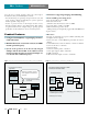
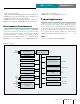
Dual-Operation Flash Memory
(Upper Bank)
Dual-Operation Flash Memory
(Lower Bank)
SA9:4K-byte
Write/erase available in one bank
while a program is executed in the
other bank
SA8:4K-byte
SA3:4K-byte
Dual-Operation
Read (Execution)
Write/Erase
Write/Erase
Read (Execution)
OR
CPU
SA2:4K-byte
SA1:4K-byte
SA0:4K-byte
SA7:4K-byte
SA6:4K-byte
SA5:16K-byte
SA4:16K-byte
Figure 1
Operation of Dual-Operation Flash Memory-Integrated Microcontroller Series MB90F897
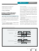
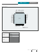
Flash
Memory
RAM
CPU
①
①Rewriting from flash memory
to RAM Program transmission
Existing Flash Memory
No need to transfer programs to RAM
when flash memories rewrite.
Dual-Operation Flash Memory
②Rewriting to flash memory
②
Upper Bank
Lower Bank
Flash Memory
CPU
①
①Rewriting to flash memory
①
Figure 2 Operational Flow of CPU Rewrite by Flash Memory