LSI Specification MB86617A IEEE1394 Serial Bus Controller for DTV MB86617A LSI Specification Rev. 1.0 Rev.1.
LSI Specification MB86617A Contents CHAPTER 1 OVERVIEW ............................................................................................................................................................................1 CHAPTER 2 FEATURES ..............................................................................................................................................................................2 CHAPTER 3 CHIP BLOCK .................................................................
LSI Specification MB86617A 7.3. INSTRUCTION FETCH R EGISTER ........................................................................................................................................................... 31 7.4. INTERRUPT-FACTOR INDICATE REGISTER/ INTERRUPT-MASK SETTING REGISTER........................................................................ 32 7.5. R ECEIVE A CKNOWLEDGE INDICATE R EGISTER .................................................................................................
LSI Specification MB86617A 7.32. PING T IME M ONITOR REGISTER ........................................................................................................................................................ 70 7.33. PHY/LINK REGISTER/A DDRESS SETTING REGISTER ................................................................................................................... 71 7.34. PHY/LINK REGISTER ACCESS P ORT ......................................................................................
LSI Specification MB86617A 9.2. DESCRIPTION OF EACH INSTRUCTION............................................................................................................................................... 103 CHAPTER 10 INTERRUPT ..................................................................................................................................................................... 106 10.1. I NTERRUPT-FACTOR I NDICATOR REGISTER & INTERRUPT- MASK SETTING REGISTER .............................
LSI S pecification MB86617A Chapter 1 Overview This chapter explains the overview of MB86617A. MB86617A is Fujitsu’s IEEE1394 serial bus controller based on both IEEE1394 Standard (IEEE Std. 1394-1995) and P1394.a Standard Draft (rev.2.0). This MB86617A has three ports for network under the 1394 cable environment, differential transceiver, and comparator, and the transfer data rate supports S400.
LSI S pecification MB86617A Chapter 2 Features This chapter explains the features of MB86617A. > Compliant with IEEE1394 high performance serial bus standard and P1394.
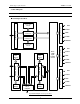
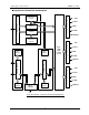
LSI S pecification MB86617A Chapte r 3 Chip Block This chapter explains the MB86617A block diagram and the function of each block. 3.1. Block Diagram 3.2. Function of Each Block Rev.1.
LSI S pecification MB86617A 3.1. Block Diagram MB86617A block diagram is shown below.
LSI S pecification MB86617A < Asynchronous Transmit FIFO Extended Mode Asynch Transmit Exclusive FIFO (256 byte) TPA0 1394 Interface (Port 0) Host Interface Asynch Transmit PacketProcess Asynch Transmit PacketProcess XTPA0 TPB0 XTPB0 TPBIAS0 Asynch Transmit Exclusive FIFO (256 byte) TPA1 FIFO (2KByte) CP IC Interface FIFO (2KByte) XTPA1 TPB1 XTPB1 TPBIAS1 TPA2 1394 Interface (Port 2) (2KByte) Data Bridge TSP IC Interface FIFO 1394 Interface (Port 1) FIFO (2KByte) PHY/ LINK Layer Control C
LSI S pecification MB86617A < Asynchronous Receive FIFO Extended Mode Asynch Transmit Exclusive FIFO (256 byte) TPA0 1394 Interface (Port 0) Host Interface Asynch Transmit Packet Process Asynch Transmit Packet Process XTPA0 TPB0 XTPB0 TPBIAS0 Asynch Transmit Exclusive FIFO (256 byte) TPA1 FIFO (2KByte) CP IC Interface FIFO (2KByte) XTPA1 TPB1 XTPB1 TPBIAS1 TPA2 1394 Interface (Port 2) (2KByte) Data Bridge TSP IC Interface FIFO 1394 Interface (Port 1) FIFO (2KByte) PHY/ LINK Layer Control
LSI S pecification MB86617A 3.2. Function of Each Block This section explains the function of each block for MB86617A. < PHY Layer Control Circuit This circuit is for the Physical layer of IEEE 1394 with the following functions. > Asynchronous transfer is supported under cable environment. > Maximum transfer data rate : 393.216Mbit/sec.
LSI S pecification MB86617A Chapter 4 Pin Assignment This chapter explains the pin assignment and table of pin function of MB86617A. 4.1. Pin Assignment 4.2. Corresponding Table of MB86617A Pin 4.3. Outline Drawing of Package Rev.1.
LSI S pecification MB86617A 4.1. Pin Assignment The following diagram shows the MB86617A pin assignment.
LSI S pecification MB86617A 4.2. Corresponding Table of MB86617A Pin The following table shows the corresponding items of MB86617A pin. Pin No. I/O Pin Name Pin No.
LSI S pecification MB86617A 4.3. Outline Drawing of Package This section shows the outline drawing of MB86617A package (LQFP -176). Rev.1.
LSI S pecification MB86617A Chapter 5 Pin Function This chapter explains the MB86617A pin function. 5.1. IEEE1394 Interface 5.2. Isochronous (TSP-IC,DV-IC) Interface 5.4. MPU Interface 5.5. Other Pins 5.6. Power/GND Pin Rev.1.
LSI S pecification MB86617A 5.1. IEEE1394 Interface This section explains the pin function of IEEE1394 interface.
LSI S pecification MB86617A 5.2. Isochronous Interface This section explains the pin function of Isochronous interface. Signal Name I/O TSVALIDA I/O I.
LSI S pecification MB86617A IERRA O IERRB O Output pin for noticing error of receive data (on port A) ‘H’ active signal Output pin for noticing error of receive data (on port B) ‘H’ active signal DSSCLKA I Clock input pin for DSS data (27MHz) DSSCLKB I Clock input pin for DSS data (27MHz) Rev.1.
LSI S pecification MB86617A 5.4. MPU Interface This section explains the pin function of MPU interface.
LSI S pecification MB86617A 5.5. Other Pins This section explains the pin function like internal PLL. Signal Name I/O XRESET I Input signal for resetting signal When operating with cable supply power, set this pin to ‘L’. I This pin is used for setting operating mode of MPU.
LSI S pecification MB86617A 5.6. Power/GND Pin This section explains the power/GND pin. Signal Name I/O VDD - 3.3V digital power pin VSS - Digital ground pin AVDD - 3.3V analog power pin AVSS - Analog ground pin Rev.1.
LSI S pecification MB86617A Chapter 6 Internal Register This chapter explains the MB86617A internal register. Note that the access of internal register is applied only 16 bits access.
LSI S pecification MB86617A WRITE READ Register Name Register Name 20 transmit DSS packet header setting [A] (upper) receive DSS packet header setting [A] (upper) 22 transmit DSS packet header setting [A] (medium) receive DSS packet header setting [A] (medium) 24 transmit DSS packet header setting [A] (lower) receive DSS packet header setting [A] (lower) 26 transmit DSS packet header setting [A] (least significant) receive DSS packet header setting [A] (least significant) 28 transmit DSS
LSI S pecification MB86617A WRITE READ Register Name Register Name 50 (reserved) data bridge transmit/receive status [B] 52 (reserved) Isochronous channel monitor 1 54 (reserved) Isochronous channel monitor 2 56 (reserved) Isochronous channel monitor 3 58 (reserved) Isochronous channel monitor 4 5A (reserved) cycle-time-monitor (upper) 5C (reserved) cycle-time-monitor (lower) 5E (reserved) Ping time monitor 60 PHY/LINK register address setting PHY/LINK register address settin
LSI S pecification MB86617A WRITE READ Register Name Register Name 80 (reserved) transmit CGMS/TSCH indicate [A] 82 (reserved) transmit CGMS/TSCH indicate [B] 84 transmit CGMS/TSCH indicate status transmit CGMS/TSCH indicate status 86 transmit EMI/OE setting transmit EMI/OE setting 88 (reserved) (reserved) 8A (reserved) (reserved) 8C (reserved) (reserved) 8E (reserved) (reserved) 90 (reserved) (reserved) 92 (reserved) (reserved) 94 (reserved) (reserved) 96 (reserved)
LSI S pecification MB86617A WRITE READ Register Name Register Name B0 (reserved) (reserved) B2 (reserved) (reserved) B4 (reserved) (reserved) B6 (reserved) (reserved) B8 (reserved) (reserved) BA (reserved) (reserved) BC (reserved) (reserved) BE (reserved) (reserved) C0 (reserved) (reserved) C2 (reserved) (reserved) C4 (reserved) (reserved) C6 (reserved) (reserved) C8 (reserved) (reserved) CA (reserved) (reserved) CC (reserved) (reserved) CE (reserved) (re
LSI S pecification MB86617A WRITE READ Register Name Register Name E0 (reserved) (reserved) E2 (reserved) (reserved) E4 (reserved) (reserved) E6 (reserved) (reserved) E8 (reserved) (reserved) EA (reserved) (reserved) EC (reserved) (reserved) EE (reserved) (reserved) F0 (reserved) (reserved) F2 (reserved) (reserved) F4 (reserved) (reserved) F6 (reserved) (reserved) F8 (reserved) (reserved) FA (reserved) (reserved) FC (reserved) (reserved) FE (reserved) (re
LSI S pecification MB86617A Chapter 7 Internal Register Function Description This chapter explains the details of the internal register of MB86617A. 7.1. mode-control Register 7.2. flag & status Register 7.3. instruction fetch Register 7.4. interrupt-factor Indicate Register/interrupt-mask Setting Register 7.5. Receive Acknowledge Indicate Register 7.6. A-buffer Data Port Receive/Transmit 7.7. TSP Transmit Information Setting Register [A] 7.8. TSP Transmit Information Setting Register [B] 7.9.
LSI S pecification 7.25. 7.26. 7.27. 7.28. 7.29. 7.30. 7.31. 7.32. 7.33. 7.34. 7.35. 7.36. 7.37. 7.38. 7.39. Rev.1.
LSI S pecification MB86617A 7.1. M ode-control Register Mode-control register is the register that performs the relative setting of various operation mode of this LSI.
LSI S pecification MB86617A BIT Bit Name Action 3 Asyn-FIFO sel Read/ Write 2 1 0 send/rec TSP stand-by CP stand-by value Function 0 Uses 2K byte FIFO on LINK I/F side of bridge for Isochronous transmit/receive. 1 Uses 2K byte FIFO on LINK I/F side of bridge for Asynchronous transmit/receive. 0 Uses 2K byte FIFO for Asynchronous transmit with Asyn-FIFO sel (bit3) ‘1’. 1 Uses 2K byte FIFO for Asynchronous receive with Asyn-FIFO sel (bit3) ‘1’. 0 Activates TSP -IC I/F terminal output.
LSI S pecification MB86617A 7.2. flag & status Register flag & status register indicates the status of this LSI and data access inquiries.
LSI S pecification BIT 4 3 2 1 0 Bit Name sleep data req recv busy Note 2) cmstr INT MB86617A Action Value Function 0 Indicates that the device is not in forced sleep. 1 Indicates that the device is in forced sleep by accepting “Start sleep” (01h) instruction. 0 Indicates that no data is stored in ASYNC receive specific buffer. 1 Indicates that data is stored in ASYNC receive specific buffer. 0 Indicates that packet receive is not in busy mode.
LSI S pecification MB86617A 7.3. instruction-fetch Register instruction-fetch register is the register that writes in instructions for this LSI, and consists of the instruction code and operand. Refer to “Chapter 9 Instruction” for each instruction code and operand code.
LSI S pecification MB86617A 7.4. interrupt-factor Indicate Register/interrupt-mask Setting Register interrupt-factor indicate register is the register that indicates interrupt reported by this LSI. Refer to “Chapter 10 Interrupt” for measure against and details of each Bit and interrupt factor. interrupt-mask setting register is the register that controls mask of each interrupt factor generated by this LSI.
LSI S pecification MB86617A 7.5. Receive Acknowledge Indicate Register Receive Acknowledge indicate register is the register that indicates received Acknowledge packet addressed to itself. Read out this register after interrupt report of “Asynchronous packet send”.
LSI S pecification MB86617A 7.6. A-buffer Data Port Receive/Transmit This integrated register is the buffer access port for both ASYNC receive specific buffer and ASYNC transmit specific one. Read data is able to be read out IEEE1394 packet data in the order received. (MSB: 1 ST read) Write data is transmitted as IEEE1394 packet data in the order written in.
LSI S pecification MB86617A 7.7. TSP Transmit Information Setting Register [A] TSP transmit information setting register [A] is the register that makes settings for transmit packet processed by bridge-Ach. AD R/W Bit 15 Bit 14 Bit 13 10h R/W Tx start -A Tx end -A Tx select -A Initial Value ‘0’ ‘0’ ‘0’ BIT 15 14 13 Bit 12 Bit Name Action Tx start -A Read/ Write Tx end-A Tx select-A Read/ Write Read/ Write 12 - 7 set TS-ID-A Read/ Write 6 Tx form-A Read/ Write 5 Rev.1.
LSI S pecification BIT 4 3- 2 1 0 Rev.1.0 Bit Name EMI select-A set EMI-A 27M count-A port mask -A MB86617A Action Value Function 0 Selects CGMS information input from TSP -IC as EMI information to be output to CP-IC. 1 Selects setting value of set EMI-A (bit3 to 2) as EMI information to be output to CP-IC. - Set EMI information to be output to CP-IC. Valid only when EMI select -A (bit4) is ‘1’.
LSI S pecification MB86617A 7.8. TSP Transmit Information Setting Register [B] TSP transmit information setting register [B] is the register that makes settings for transmit packet processed by bridge-Bch. AD R/W Bit 15 Bit 14 Bit 13 12h R/W Tx start -B Tx end -B Tx select -B Initial Value ‘0’ ‘0’ ‘0’ BIT 15 14 13 Bit 12 Bit Name Action Tx start -B Read/ Write Tx end-B Tx select-B Read/ Write Read/ Write 12 - 7 set TS-ID-B Read/ Write 6 Tx form-B Read/ Write 5 Rev.1.
LSI S pecification BIT 4 3- 2 1 0 Rev.1.0 Bit Name EMI select-B set EMI-B 27M count-B port mask -B MB86617A Action Value Function 0 Selects CGMS information input from TSP -IC as EMI information to be output to CP-IC. 1 Selects setting value of set EMI-A (bit3 to 2) as EMI information to be output to CP-IC. - Set EMI information to be output to CP-IC. Valid only when EMI select -A (bit4) is ‘1’.
LSI S pecification MB86617A 7.9. Transmit Offset Setting Register [A] Transmit offset setting register [A] is the register that sets offset value added to cycle-time-monitor value. Its aim is to generate source packet header (Time-stamp) added to transmit packet processed by bridge -Ach. (Max. 32 ms) Time-stamp value is generated on the basis of cycle-time-monitor value at input of first byte of source packet from TSP -IC.
LSI S pecification MB86617A 7.10. Transmit Offset Setting Register [B] Transmit off set setting register [B] is the register that sets offset value added to cycle-time-monitor value Its aim is to generate source packet header (Time-stamp) added to transmit packet processed by bridge -Bch. (Max. 32 ms) Time-stamp value is generated on the basis of cycle-time-monitor value at input of first byte of source packet from TSP -IC.
LSI S pecification MB86617A 7.11. TSP Receive Information Setting Register TSP receive information setting register performs the setting for outputting received packet to TSP -IC AD R/W Bit 15 Bit 14 Bit 13 Bit 12 Bit 11 Bit 10 Bit 9 Bit 8 1Ch R/W TV2B TV1B - - output DSS size-B DVEN DSSEN TS-E N ‘0’ ‘0’ ‘0’ ‘0’ ‘0’ ‘0’ ‘0’ ‘1’ Initial Value BIT 15 14 13 - 12 11 10 9 Rev.1.
LSI S pecification BIT 8 7 6 5- 4 3 2 1 0 Bit Name TS-EN TV2A TV1A MB86617A Action Value Function 0 Deletes received data and reports FMT error when MPEG2 -TS data is received. ISO packet header and CIP header are indicated in register. 1 Allows receiving MPEG2 -TS data. 0 Does not output the packet received by bridge-Ach to port B of TSP-IC I/F. 1 Outputs the packet received by bridge-Ach to port B of TSP -IC I/F.
LSI S pecification MB86617A Register setting value and selection of output port are shown in the table below.
LSI S pecification MB86617A 7.12. Receive DSS Packet Header Indicate Register [A]/Transmit DSS Packet Header Setting Register [A] Receive DSS packet header indicate register [A] indicates DSS packet header range of DSS packet received by bridge-Ach. Transmit DSS packet header setting register [A] sets DSS packet header range of DSS packet received by bridge -Ach.
LSI S pecification MB86617A 7.13. Receive DSS Packet Header Indicate Register [B]/Transmit DSS Packet Header Setting Register [B] Receiv e DSS packet header indicate register [B] indicates DSS packet header range of DSS packet received by bridge-Bch. Transmit DSS packet header setting register [B] sets DSS packet header range of DSS packet received by bridge-Bch.
LSI S pecification MB86617A 7.14. TSP Status Register TSP status register indicates status of TSP -IC I/F.
LSI S pecification MB86617A BIT Bit Name Active Value 9~8 reserved Read - Always indicate ‘0’. 0 Indicates that CGMS information input from port A of TSP IC I/F is not changed. 1 Indicates that CGMS information input from port A of TSP IC I/F is changed. Clears to ‘0’ by lead of this register. 0 Indicates that TS classification ID input from port A of TSP IC I/F is not changed.
LSI S pecification MB86617A 7.15. Data Bridge Transmit Information Setting Register 1 [A] Data bridge transmit information setting register 1 [A] is the register that sets CIP header range added to transmit packet processed by bridge-Ach.
LSI S pecification MB86617A 7.16. Data Bridge Transmit Information Setting Register 2 [A] Data bridge transmit information setting register 2 [A] is the register that sets CIP header range, transmit channel, and speed added to transmit packet processed by bridge-Ach.
LSI S pecification MB86617A 7.17. Data Bridge Transmit Information Setting Register 3 [B] Data bridge transmit information setting register 3 [B] is the register that sets CIP header range added to transmit packet processed by bridge-Bch.
LSI S pecification MB86617A 7.18. Data Bridge Transmit Information Setting Register 4 [B] Data bridge transmit information setting register 4 [B] is the register that sets CIP header range, transmit channel and speed added to transmit packet processed by bridge-Bch.
LSI S pecification MB86617A 7.19. Data Bridge Receive Information Setting Register Data bridge receive information register performs the setting of receive packet. AD R/W Bit 15 Bit 14 3Ch R/ Rx start -B Rx end -B ‘0’ ‘0’ Initial Value BIT 15 14 13~8 7 6 5- 0 Rev.1.
LSI S pecification MB86617A 7.20. Transmit Packet Link/Split Setting Register Transmit packet link/split setting register is the register that sets number of link and split of source packets to be transmitted.
LSI S pecification BIT 5 Bit Name NF5SPA MB86617A Action Read/ Write Value Function 0 Executes 2SP combined transmission as FIFO NFULL operation when setting of 2SP separated transmission or combined transmission for less than 2SP. With more than 3 SP, executes according to setting. 1 Executes 5 SP combined transmission at FIFO FULL. 4- 2 SPQA Read/ Write - Write in number of links for source packet processed by bridge-Ach.
LSI S pecification MB86617A 7.21. Late Packet Decision Range Setting Register [A] Late packet decision range setting register [A] is the register that sets Late decision range of source packet to be transmitted by bridge -Ach. AD R/W 40h R/W Bit 15 Bit 14 Bit 13 Bit 12 Bit 11 Bit 10 Bit 9 Bit 8 Bit 5 Bit 4 Bit 3 Bit 2 Bit 1 Bit 0 “0000 h ” Bit Name Action Value Function Write in Late packet decision range. Setting range is 0h to FFh (unit: 125µS).
LSI S pecification MB86617A 7.22. Late Packet Decision Range Setting Register [B] Late packet decision range setting register [B] is the register that sets Late decision range of source packet to be transmitted by bridge -Bch. AD R/W 42h R/W Bit 15 Bit 14 Bit 13 Bit 12 Bit 11 Bit 10 Bit 9 Bit 8 Bit 5 Bit 4 Bit 3 Bit 2 Bit 1 Bit 0 “0000 h ” Bit Name Action Value Function Write in Late packet decision range. Setting range is 0h to FFh (unit: 125µS).
LSI S pecification MB86617A 7.23. Receiv e Isochronous Packet Header Indicate Register 1 [A] Receive Isochronous packet header indicate register 1 [A] is the register that indicates Isochronous packet header information received by bridge-Ach.
LSI S pecification MB86617A 7.24. Receive Isochronous Packet Header Indicate Register 2 [A] Receive Isochronous packet header indicate register 2 [A] is the register that indicates Isochronous packet CIP header information received by bridge-Ach.
LSI S pecification MB86617A 7.25. Receive Isochronous Packet Header Indicate Register 3 [B] Receive Isochronous packet header indicate register 3 [B] is the register that indicates Isochronous packet header information received by bridge-Bch.
LSI S pecification MB86617A 7.26. Receive Isochronous Packet Header Indicate Register 4 [B] Receive Isochronous packet header indicate register 4 [B] is the register that indicates Isochronous packet CIP header information received by bridge-Bch.
LSI S pecification MB86617A 7.27. FIFO Reset Setting Register FIFO reset setting register sets force reset of bridge and each FIFO.
LSI S pecification MB86617A 7.28. Data Bridge Transmit/Receive Status Register [A] Data bridge transmit/receive status register indicates status of packet to be transmitted/received by bridge-Ach. AD R/W Bit 15 Bit 14 Bit 13 Bit 12 Bit 11 Bit 10 R Tx busyA Rx busyA Rx 1STPA Rx EMI chg-A Rx o/e chg-A ‘0’ ‘0’ ‘0’ ‘0’ ‘0’ 4Eh Initial Value BIT 15 14 13 12 11 Rev.1.
LSI S pecification BIT 10 9 8 7 6 5 4 3 2 Rev.1.0 Bit Name Rx dlen-err-A reserved Tx late-A Rx late-A Rx 56 err-A Rx stype err-A BRG FIFO full-A BRG FIFO emp-A Rx DBC err-A MB86617A Action Value Function 0 Indicates that the data length of received packet is same as specified data length in format. 1 Indicates that the data length of received packet differs to the specified data length in the format. Clears to ‘0’ by lead of this register. - Always indicates ‘0’.
LSI S pecification BIT 1 0 Rev.1.0 Bit Name Rx CIP err-A Rx FMT err-A MB86617A Action Value Function 0 Indicates that CIP header of received Isochronous packet is normal. 1 Indicates that CIP header of received Isochronous packet has an error. Clears to ‘0’ by lead of this register. 0 Indicates that FMT range of CIP header of received Isochronous packet is the value allowed to be received at DV-EN, DSS- EN or TS-EN (1Ch –bit10 to 8) (DV=‘00000’, MPEG2=‘10000’ or DSS=‘100001’).
LSI S pecification MB86617A 7.29. Data Bridge Transmit/Receive Status Register [B] Data bridge transmit/receive status register [B] indicates status of packet transmitted/received by bridge-Bch. AD R/W Bit 15 Bit 14 Bit 13 Bit 12 Bit 11 Bit 10 R Tx busyB Rx busyB Rx 1STPB Rx EMI chg-B Rx o/e chg-B ‘0’ ‘0’ ‘0’ ‘0’ ‘0’ 50h Initial Value BIT 15 14 13 12 11 Rev.1.
LSI S pecification BIT 10 9 8 7 6 5 4 3 2 Rev.1.0 Bit Name Rx dlen-err-B Reserved Tx late-B Rx late-B Rx 56 err-B Rx stype err-B BRG FIFO full-B BRG FIFO emp-B Rx DBC err-B MB86617A Action Value Function 0 Indicates that data length of receive packet is same as specified data length in format. 1 Indicates that data length of receive packet differs to the specified data length in the format. Clears to ‘0’ by lead of this register. - Always indicates ‘0’.
LSI S pecification BIT 1 0 Rev.1.0 Bit Name Rx CIP err-B Rx FMT err-B MB86617A Action Value Function 0 Indicates that CIP header of received Isochronous packet is normal. 1 Indicates that CIP header of received Isochronous packet has an error. Cleared to ‘0’ by lead of this register. 0 Indicates that FMT range of CIP header of received Isochronous packet is the value allowed to be received at DV-EN, DSS- EN or TS-EN (1Ch –bit10 to 8) (DV=‘00000’, MPEG2=‘10000’ or DSS=‘100001’).
LSI S pecification MB86617A 7.30. Isochronous Channel Monitor Register Isochronous channel monitor register is the register that indicates Isochronous packet channel flowing through 1394 bus. Bit 15 Bit 14 Bit 13 Bit 12 Bit 11 Bit 10 Bit 9 Bit 8 Bit 7 Bit 6 AD R/W 52h R Isochronous channel monitor1 54h R Isochronous channel monitor2 56h R Isochronous channel monitor3 58h R Isochronous channel monitor4 Initial Value BIT 15 - 0 Rev.1.
LSI S pecification MB86617A 7.31. Cycle-timer-monitor Indicate Register Cycle-timer-monitor indicate register indicates value of integrated cycle-timer register. Bit 15 Bit 14 Bit 13 Bit 12 Bit 11 Bit 10 Bit 9 Bit 8 Bit 7 Bit 6 AD R/W 5Ah R cycle-timer-monitor (hi) 5Ch R cycle-timer-monitor (lo) Initial Value Bit 5 Bit 4 Bit 3 Bit 2 Bit 1 Bit 0 “0000 h” BIT Bit Name Action Value 15 - 0 cycle-timer-m onitor Read - Function Indicate value of built-in cycle-timer register.
LSI S pecification MB86617A 7.32. Ping Time Monitor Register Ping time monitor register is the register that indicates time period of transmitting request packet to receiving response packet to the request.
LSI S pecification MB86617A 7.33. PHY/LINK Register/Address Setting Register PHY/LINK register/address setting register is the register that sets address in order to access PHY/LINK register indirectly. PHY/LINK register indicated with address set by this register can be accessed from PHY/LINK register/access port.
LSI S pecification MB86617A 7.34. PHY/LINK Register Access Port PHY/LINK register access port is the port to access PHY/LINK register indirectly. PHY/LINK register indicated with address set by PHY/LINK register/address setting register can be accessed from this port. AD R/W 62h R/W Bit 15 Bit 14 Bit 13 Bit 12 Bit 11 Bit 10 Bit 9 Bit 8 15 - 0 Rev.1.
LSI S pecification MB86617A 7.35. Revision Indicate Register Revision indicate register is the register that indicates chip revision of this LSI. AD R/W Bit 15 Bit 14 Bit 13 Bit 12 Bit 11 64h Bit 10 Bit 9 Bit 8 Bit 7 Bit 6 Bit 5 Bit 4 Bit 3 Bit 2 Bit 1 Bit 0 Revision code (hi) 66h R Revision code (lo) Initial Value Fixed BIT Bit Name Action Value 15 - 0 Revision code Read - Rev.1.0 Function Indicate Revision code.
LSI S pecification MB86617A 7.36. Transmit CGMS/TSCH Indicate Register [A] Transmit CGMS/TSCH indicate register [A] indicates CGMS information and identification of TS type for source packet input from port A at TSP IC I/F.
LSI S pecification MB86617A 7.37. Transmit CGMS/TSCH Indicate Register [B] Transmit CGMS/TSCH indicate register [B] indicates CGMS information and identification of TS type for source packet input from port B at TSP IC I/F.
LSI S pecification MB86617A 7.38. Transmit CGMS/TSCH Indicate Status Register Transmit CGMS/TSCH indicate status register indicates validity of source packet input from TSP IC I/F.
LSI S pecification BIT Bit Name MB86617A Action Value Function 0 Indicates that the packet indicated in CGMSA-1 and TSCHA-1 (80h - bit7 to 0) was finally input from port A at TSP IC I/F. 1 Indicates that the packet indicated in CGMSA-2 and TSCHA-2 (80h- bit15 to 8) was finally input from port A at TSP IC I/F. - Clears to ‘0’ by writing “1”. 0 Indicates that the value indicated in CGMSA-2 and TSCHA-2 (80h- bit15 to 8) is invalid.
LSI S pecification MB86617A 7.39. Transmit EMI/OE Setting Register Transmit EMI/OE setting register sets EMI information and Odd/Even value added to empty packet until valid data is transmitted. AD R/W Bit 15 86h R/W IPH select -B ‘0’ Initial Value BIT 15 14 - 13 12 11 - 8 7 Rev.1.
LSI S pecification BIT Bit Name MB86617A Action Value Function - Set EMI information which are set in IPH of empty packet transmitted from bridge-Ach. Valid only when IPH select-A (bit7) is set to ‘1’. (MSB: bit6, LSB: bit5) EMI information after transmitting valid data depends on the setting of EMI select-A (10h-bit4). IPH EMI-A Read/ Write 4 IPH OE-A Read/ Write - Set Odd/Even value which is set in IPH of empty packet transmitted from bridge-Ach.
LSI S pecification MB86617A Chapter 8 PHY/INK Register Function Description This chapter explains the Physical Register and Link register that enables to access from PHY/LINK register access port (address 62h) by setting PHYT/LINK register address setting register (address 60h) in detail. 8.1. 8.2. 8.3. 8.4. 8.5. 8.6. 8.7. 8.8. 8.9. 8.10. 8.11. 8.12. 8.13. 8.14. 8.15. 8.16. 8.17. 8.18. Rev.1.
LSI S pecification MB86617A 8.1. PHY/LINK Register Table Table of Physical Register and Link Register is shown below.
LSI S pecification MB86617A PHY/LINK addr Write Read 2Ch Physical register #17 ← 2Eh Physical register #18 ← 30h Physical register #19 ← 32h Physical register #1A ← 34h Physical register #1B ← 36h Physical register #1C ← 38h Physical register #1D ← 3Ah Physical register #1E ← 3Ch Link register #00 ← 3Eh Link register #01 ← 40h Link register #02 ← 42h Link register #03 ← Rev.1.
LSI S pecification MB86617A 8.2. Physical register #00 (read) Physical Register#00 is the register that indicates Physical ID, root status, and cable power st atus of this node.
LSI S pecification MB86617A 8.3. Physical register #01 (read/write) Physical Register#01 is the register that set s/indicates force-root and gap-count. Do not write into this register except for the case that the node is Bus manager or Isochronous resource manager in the environment with no Bus manager.
LSI S pecification MB86617A 8.4. Physical register #02 (read) Physical Register#02 is the register that indicates if the extended PHY register map is in existence or not, and the number of ports (3 port).
LSI S pecification MB86617A 8.5. Physical register #03 (read) Physical Register#03 is the register that indicates max. transfer speed (S400) of this node.
LSI S pecification MB86617A 8.6. Physical register #04 (read/write) Physical Register#04 is the register that sets the parameter of Self-ID packet to be transmitted by this node.
LSI S pecification MB86617A 8.7. Physical register #05 (read/write) Physical Register#05 is the register indicating availability of cable supply power standard and timeout detect of arbitration state machine.
LSI S pecification BIT Bit Name MB86617A Action Value 0 Indicates that port event and resume processing have not occurred. 1 Indicates that Connected, Bias, Disabled, Fault bit has changed when Int_enable bit is set at ‘1’. Indicates that resume processing was performed when Resume_Int bit is set at ‘1’. - Clears the bit value to ‘0’ by writing in ‘1’. 0 Disables arbitration acceleration function. 1 Enables arbitration acceleration function.
LSI S pecification MB86617A 8.8. Physical register #07, 08, 09 (read) Physical Register#07, 08, 09 are the registers that indicate signal condition of IEEE1394 port and cable connection condition.
LSI S pecification MB86617A 8.9. Physical register #0A, 0B, 0C (read/write) Physical Register#0A, 0B, 0C are the registers that indicate bias detect condition of IEEE1394 installed in this node and performs setting of enable/disable of IEEE1394 port.
LSI S pecification MB86617A 8.10. Physical register #0D, 0E, 0F (read/write) Physical Register#0D, 0E, 0F are the registers that indicate maximum transfer speed of the node connected to IEEE1394 port installed in this node.
LSI S pecification MB86617A 8.11. Physical register #10 (read) Physical Register#10 is the register that indicates Compliance_level of this node. phy/ linkaddr R/W Bit 15 Bit 14 Bit 13 Bit 12 Bit 11 Bit 10 Bit 9 Bit 8 1E h R - - - - - - - - Compliance_level ‘0’ ‘0’ ‘0’ ‘0’ ‘0’ ‘0’ ‘0’ ‘0’ “01 h” Fixed value Bit 7 Bit 6 Bit 5 Bit 4 Bit 3 Bit 2 Bit 1 Bit 0 Description of Each Bit BIT Bit Name Action Value 15 - 8 reserved Read - Always indicate ‘0’.
LSI S pecification MB86617A 8.12. Physical register #11, 12, 13 (read) Physical Register#11, 12, 13 are the registers that indicate Vendor_ID of this node.
LSI S pecification MB86617A 8.13. Physical register #14, 15, 16 (read) Physical Register#14, 15, 16 are the registers that indicate Product_ID of this node.
LSI S pecification MB86617A 8.14. Physical register #17, 18, 19, 1A, 1B, 1C, 1D, 1E (read/write) Physical Register#17, 18, 19, 1A, 1B, 1C, 1D, 1E are in the range of 8 bit X 8 Free_RAM.
LSI S pecification MB86617A 8.15. Link register #00 (read/write) Link Register#00 is the register that sets this node to operate as cycle master.
LSI S pecification MB86617A 8.16. Link register #01 (read/write) Link Register#00 is the register that sets this node to perform as cycle master.
LSI S pecification MB86617A 8.17. Link register #02 (read/write) Link Register#02 is the register that sets transfer mode of acknowledge packet transmitted by this node and disable setting of Link layer.
LSI S pecification MB86617A 8.18. Link register #03 (read/write) Link Register#03 is the register that performs Link layer reset and initializes setting of the node.
LSI S pecification MB86617A Chapter 9 Instruction This chapter explains the instruction codes and details for respective instructions. 9.1. 9.2. Rev.1.
LSI S pecification MB86617A 9.1. Instruction Code Table Instruction name code Operand Start sleep 01 Remove sleep 02 Asynchronous receive 03 Remove busy mode 04 Send PHY packet 21 Asynchronous Send 31 Speed code Data-FIFO init 63 FIFO select code DMA Transmit (Asynchronous) 71 DMA Transmit (PHY packet) 72 DMA Receive 73 Rev.1.
LSI S pecification MB86617A 9.2. Description of Each Instruction < Start sleep (01 h) This instruction changes this device into forced sleep, stops the driver/receiver function of 1394 port, and then changed into the status with this device’s cable cut. Also, it stops the clock to be input from integrated PLL to IEEE1394 block. Access to each register is available. No interrupt this instruction is reported. Confirm the sleep condition using sleep Bit (Bit4) of flag & status register (address 02h).
LSI S pecification MB86617A < Asynchronous Send (31 h) This instruction transmits the data stored at the ASYNC transmit specific buffer. This instruction performs the following serial actions, from access to arbitration by detecting arb-reset-gap, generation and transfer of packet, to receipt of Acknowledge packet. When the performances from packet transmit to Acknowledge receive are normally completed, this instruction reports interrupt of “Asynchronous packet send” (INT17).
LSI S pecification MB86617A < DMA Transmit (Asynchronous) (71h) This instruction writes in the transmit Asynchronous packet to ASYNC transmit specific buffer using DMA transmit. Assert DREQ signal after issuing this instruction. Determine the transmit bite value by transmit data length within packet header, write in up to quadlet unit, then negate DREQ signal. After completion of writing in, issue the Asynchronous send instruction (31h).
LSI S pecification MB86617A Chapter 10 Interrupt This chapter explains the inturrput-factors and method for interrupt-mask. 10.1. 10.2. 10.3. Rev.1.
LSI S pecification MB86617A 10.1.
LSI S pecification MB86617A 10.2. Interrupt Interrupt INT1 INT2 INT3 INT4 INT5 INT6 INT7 INT8 INT9 INT10 INT11 INT12 INT13 INT14 INT15 INT16 INT17 INT18 INT19 INT20 INT21 INT22 INT23 INT24 INT25 INT26 INT27 INT28 INT29 INT30 INT31 INT32 Rev.1.
LSI S pecification MB86617A 10.3. Description of Interrupt Each interrupt items are described below. Interrupt INT1 Interrupt Item Loop detected Description Topology is in Loop. > Need to issue “Bus reset”. Occurred convention failure like Physical-ID did not count up each Self-ID packet received during Self Identify process. > Continues to receive Self-ID packet after reporting interrupt, but reports “Bus reset complete” (05h) interrupt.
LSI S pecification Interrupt MB86617A Interrupt Item Description INT7 Isochronous cycle too long Isochronous cycle exceeded specified time. >Informs only if this node is Cycle master. INT8 Bus occupancy violation Node occupied longer time than MAX_DATA_TIME. >Need to issue “Bus reset”. INT9 Asynchronous packet received Received Asynchronous packet addressed to self-node normally, and stored data at ASYNC receive specific buffer.
LSI S pecification Interrupt MB86617A Interrupt Item Description INT23 Cycle start packet received Received cycle start packet normally when self node is not root > Isochronous cycle starts. Set ISO cycle Bit (Bit12) of flag & status register (address 02h) at ‘1’ simaltaneously with this interrupt report. INT24 Cycle start packet send Completed to send Cycle start packet when self node is root. INT25 Physical packet send Completed to send Physical packet.
LSI S pecification MB86617A Chapter 11 Operation This chapter explains the operation of this device and displays the examples of control flow. 11.1. Initialization 11.2. Self-ID Packet Receiving 11.3. Asynchronous Packet Transmitting 11.4. Asynchronous Packet Receiving 11.5. Isochronous Packet Transmitting 11.6. Isochronous Packet Receiving Rev.1.
LSI S pecification MB86617A 11.1. Initialization The example of control flow from the system power on to the packet transmitting/receiving possible state is shown below. In this examle, the device is not operated with cable power supply before turning on the power of system. START System power ON Power CPS terminal to ‘L’, up to 500ns. Power XRESET terminal to ‘L’, up to 400ns. Inner reset and release reset. Start internal PLL. Receive BUS_RESET No Yes Start bus reset process.
LSI S pecification MB86617A 11.2. Self-ID Packet Receiving The example of control flow for receiving Self -ID packet is shown below. 11.2.1 11.2.2 Rev.1.
LSI S pecification 11.2.1 MB86617A Self-ID Packet Receive at Bus Reset Process This section explains the receiving process of Self-ID packet. The MB86617A device is capable of receiving self-ID packets that each mode transmit in the self-identity stage of bus reset process. When ‘1’ is written to the s-ID store bit of mode- control register (refer to 7.
LSI S pecification MB86617A < Flow chart before bus reset completion Start bus reset. Read Bus reset detected (INT4) interrupt. Report Bus reset detected (INT4) interrupt. (assert XINT) (Assert XINT). ‘1’ -ID store ‘0’ Bus reset completed . No Yes Read Bus reset completed (INT3) interrupt. Report Bus reset completed (INT3) interrupt. END Set FIFO according to FIFO mode. Clear Asynchronous receive buffer.
LSI S pecification MB86617A < Flow chart after bus reset completion START Read Self -ID? No Yes Issue Asynchronous receive (03h) instruction. Prepare for reading received data. Read one word from receive Asynchronous data port. ‘1’ Read one word of the received data and increment the read pointer of buffer. data req bit ‘0’ Issue Remove busy (04h) instruction. Receive Remove busy(04h) instruction.
LSI S pecification 11.2.2 MB86617A Self-ID Packet Receive after Transmitting Ping Packet Ping Regardless of s-ID store bit setting in the mode- control register (refer to 7.1), the device receives self-ID packet after a ping packet transmitted and stores the data removing logical inverse section in the Asynchronous receive-FIFO. < Flow chart from transmitting of Pig packet to receiving Self-ID packet Ping START Store ping packet to be transmitted in Asynchronous receive buffer.
LSI S pecification MB86617A < Flow chart after receiving Self-ID packet START Issue Asynchronous receive (03h) instruction. Prepare for reading received data Read the data of one word from receive Asynchronous data port. Read one word of received data and increment the read pointer Of receive buffer. Read flag & status register. 1 data req bit 0 Issue Remove busy (04h) instruction. Receive Remove busy (04h) instruction. FIFO remote mode for receiving completed.
LSI S pecification MB86617A 11.3. Asynchronous Packet Transmitting The example of control flow for transmitting of Asynchronous packet is shown below. < Flow chart before storing transmitting data into Asynchronous transmit FIFO START Write data for 1 word for Asynchronous transmit buffer and increment the write pointer. Write one word the data to be transmitted in Asynchronous transmit data port. Number of residual transfer byte = Number of residual transfer byte –(minus) 2.
LSI S pecification MB86617A < Flow chart after storing transmitting data into Asynchronous transmit FIFO START Receive Asynchronous transmit (31h) instruction. Issue Asynchronous transmit (31h) instruction. Read Asynchronous transmit buffer. Arbitration procedure Arbitration result Lost Won Transmit Asynchronous packet. After the transfer of DATA_END, release bus and wait Asynchronous packet receiving.
LSI S pecification MB86617A 11.4. Asynchronous Packet Receiving The example of control flow for receiving Asynchronous packet is shown below. Rev.1.
LSI S pecification MB86617A < Flow chart for received data before storing in Asynchronous receive FIFO Receive packet to self-node. Check Header CRC. OK NG Report Header CRC Error(INT14) interrupt and duscard received packet. Read Header CRC Error (INT14) interrupt. Packet receiving process completed recv busy bit ‘0’ ‘1’ Transmit “Ack_busy_X” and discard received packet. Packet receiving process completed Store Asynchronous packet into Async hronous receive buffer.
LSI S pecification MB86617A < Flow chart for received data after storing in Asynchronous receive FIFO START Issue Asynchronous receive(03h) instruction. Prepare for reading received data. Read 1 word of the data from receive Asynchronous data port Read 1 word of received data and increment read pointer of receive buffer. Read flag & status register. 1 data req bit 0 Issue Remove busy(04h) instruction Receive Remove busy(04h) instruction. Receive FIFO read mode completed.
LSI S pecification MB86617A 11.5. Isochronous Packet Transmitting The example of control flow for transmitting Isochronous packet is shown below. Rev.1.
LSI S pecification MB86617A START Set necessary data to registers such as Bridg and TSPIF(Note). Set value to registers such as Bridge and TSPIF. Input the source packet data and clock into TSPIF port. Store source packet in FIFO at TSPIF. Transmit source packet to CP LSI. Receive processed source packet from CP LSI and store it in FIFO at Bridge.
LSI S pecification MB86617A (Note)Register and bit necessary for transmitting are as follows. Data Address 00h 14h,16h 18h,1Ah 34h 36h 38h 3Ah 40h 42h MPEG-TS DSS TSPSB=0, CPSB=0 Set value of transmit Offset(Ach). Set value of transmit Offset (Bch) DBSA=06h, FNA=3h TXFMTA=20h, TXCHA(Iso channel No.) DBSB=06h, FNB=3h TXFMTB=20h, TXCHB(Iso channel No.) Set criteria for Late packet (Ach). Set criteria for Late packet (Bch). DBSA=09h, FNA=2h TXFMTA=21h, TXCHA(Iso channel No.
LSI S pecification MB86617A 11.6. Isochronous Packet Receiving The example of control flow for receiving Isochronous packet is shown below. START Set necessary data to registers such as Bridg and TSPIF. Set value to registers such as Bridge and TSPIF(Note). Receive Iso packet. Store source packet in FIFO at Bridge. Transmit source packet to CP LSI. Receive processed source packet from CP LSI and store it in FIFO at TSPIF.
LSI S pecification MB86617A (Note)Register and bit necessary for receiving are as follows. Address 00h 1Ch 40h 42h 3Ch Rev.1.0 Data DSS MPEG-TS DV TSPSB=0, CPSB=0 TSEN=1, Set TV1A,TV1B,TV2A,TV2B according to Ch received and port. Set criteria for Late packet (Ach). Set criteria for Late packet (Bch). DSSEN=1, Set TV1A,TV1B,TV2A,TV2B according to Ch received and port. DVEN=1, Set TV1A,TV1B,TV2A,TV2B according to Ch received and port. - Ach received : RXSTA=1h, RXCHA(Iso channel No.
LSI S pecification MB86617A Chapter 12 System Configuration This chapter explains the system configuration of this chip. 12.1. Recommended Connection for 1934 Port (for one port) 12.2. Recommended Connection for Cable Power Supply 12.3. Recommended Connection for Build-in PLL Loop Filter 12.4. Configuration of Feedback Circuit at Crystal Oscillator Rev.1.
LSI S pecification MB86617A 12.1. Recommended Connection for 1934 Port (for one port) The example of recommended connection of 1934 port terminal for one port is shown below. 1 F 56 56 56 56 5.1k 250pF 5.1k ア1% Figure 12.1 Recommended connection for 1934 port (for one port) For unused 1394 port, TPBIAS should be open and TPA, XTPA, TPB and XTPB should be be connected to GND. Rev.1.
LSI S pecification MB86617A 12.2 Recommended Connection for Cable Power Supply The example of recommended connection of cable power supply for 1394 cable is shown below. Cable Power (max 33V) 510KΩ ±5% CPS 2.2uF 91KΩ ±5% Figure 12.2 Recommended connection for cable power supply Rev.1.
LSI S pecification MB86617A 12.3. Recommended Connection for Build-in PLL Loop Filter The example of recommended connection for build-in PLL loop filter is shown below. RF FIL 390Ω ±5% 5.1KΩ ±5% 3300pF ±5% Figure 12.3 Recommended connection for build-in PLL loop filter Rev.1.
LSI S pecification MB86617A 12.4. Configuration of Feedback Circuit at Crystal Oscillator The example of configuration of feedback circuit at crystal oscillator is shown below. No outside resistance is needed because the feedback resistance is built -in.??? XO XI 20pF 20pF Figure 12.4 Configuration of feedback circuit at crystal oscillator Rev.1.