C141-E104-02EN MHL2300AT, MHM2200AT, MHM2150AT, MHM2100AT DISK DRIVES PRODUCT MANUAL
FOR SAFE OPERATION Handling of This Manual This manual contains important information for using this product. Read thoroughly before using the product. Use this product only after thoroughly reading and understanding especially the section “Important Alert Items” in this manual. Keep this manual handy, and keep it carefully. FUJITSU makes every effort to prevent users and bystanders from being injured or from suffering damage to their property. Use the product according to this manual.
This page is intentionally left blank.
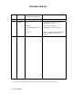
Revision History (1/1) Edition Date Revised section (*1) (Added/Deleted/Altered) Details 01 2000-02-15 — — 02 2000-09-20 -Table 1.1 - Specification (Number of Sections for MHL2300AT) was altered. - Table 1.2 - Order No. was changed. - (16) SET MAX in Section 5.3.2 - SET MAX commands are added. - Table 5.17 - Values of host termination for DIOR-, DIOW- and DMACK- signals are changed. *1 Section(s) with asterisk (*) refer to the previous edition when those were deleted.
This page is intentionally left blank.
Preface This manual describes the MHL Series and MHM Series, 2.5-inch hard disk drives. These drives have a built-in controller that is compatible with the ATA interface. This manual describes the specifications and functions of the drives and explains in detail how to incorporate the drives into user systems. This manual assumes that the reader has a basic knowledge of hard disk drives and their implementations in computer systems.
Preface Conventions for Alert Messages This manual uses the following conventions to show the alert messages. An alert message consists of an alert signal and alert statements. The alert signal consists of an alert symbol and a signal word or just a signal word. The following are the alert signals and their meanings: CAUTION IMPORTANT This indicates a hazardous situation could result in minor or moderate personal injury if the user does not perform the procedure correctly.
Preface Liability Exception “Disk drive defects” refers to defects that involve adjustment, repair, or replacement. Fujitsu is not liable for any other disk drive defects, such as those caused by user misoperation or mishandling, inappropriate operating environments, defects in the power supply or cable, problems of the host system, or other causes outside the disk drive.
This page is intentionally left blank.
Important Alert Items Important Alert Messages The important alert messages in this manual are as follows: CAUTION Task Normal Operation A hazardous situation could result in minor or moderate personal injury if the user does not perform the procedure correctly. Also, damage to the predate or other property, may occur if the user does not perform the procedure correctly. Alert message Page Data corruption: Avoid mounting the disk near strong magnetic sources such as loud speakers.
This page is intentionally left blank.
Manual Organization MHL2300AT, MHM2200AT, MHM2150AT, MHM2100AT DISK DRIVES PRODUCT MANUAL (C141-E104) • • • • • • Device Overview Device Configuration Installation Conditions Theory of Device Operation Interface Operations MHL2300AT, MHM2200AT, MHM2150AT, MHM2100AT • Maintenance and Diagnosis • Removal and Replacement Procedure DISK DRIVES MAINTENANCE MANUAL (C141-F043) C141-E104-02EN vii
This page is intentionally left blank.
Contents CHAPTER 1 Device Overview ....................................................................... 1-1 1.1 C141-E104-02EN 1-2 1.1.1 Functions and performance 1.1.2 Adaptability 1.1.3 Interface 1.2 CHAPTER 2 Features 1-2 1-2 1-3 Device Specifications 1-4 1.2.1 Specifications summary 1-4 1.2.2 Model and product number 1.3 Power Requirements 1.4 Environmental Specifications 1.5 Acoustic Noise 1.6 Shock and Vibration 1.7 Reliability 1-9 1.8 Error Rate 1-10 1.
Contents CHAPTER 3 Installation Conditions.............................................................. 3-1 3.1 Dimensions 3.2 Mounting 3.3 Cable Connections 3-10 3.3.1 Device connector 3-10 3.3.2 Cable connector specifications 3.3.3 Device connection 3.3.4 Power supply connector (CN1) 3.4 CHAPTER 4 3-4 Jumper Settings 3-11 3-11 3-12 3-12 3.4.1 Location of setting jumpers 3.4.2 Factory default setting 3.4.3 Master drive-slave drive setting 3.4.
Contents 4.6.2 Write circuit 4-11 4.6.3 Read circuit 4-13 4.6.4 Digital PLL circuit 4.7 CHAPTER 5 4-15 4.7.1 Servo control circuit 4.7.2 Data-surface servo format 4.7.3 Servo frame format 4.7.4 Actuator motor control 4.7.5 Spindle motor control 4-15 4-18 4-20 4-21 4-22 Interface..................................................................................... 5-1 5.1 Physical Interface 5-2 5.1.1 Interface signals 5-2 5.1.2 Signal assignment on the connector 5.
Contents 5.5.2.1 Ultra DMA burst initiation phase 5.5.2.2 Data transfer phase 5-93 5-94 5.5.2.3 Ultra DMA burst termination phase 5.5.3 Ultra DMA data in commands 5-94 5-95 5.5.3.1 Initiating an Ultra DMA data in burst 5.5.3.2 The data in transfer 5-95 5-96 5.5.3.3 Pausing an Ultra DMA data in burst 5-96 5.5.3.4 Terminating an Ultra DMA data in burst 5.5.4 Ultra DMA data out commands 5-100 5.5.4.1 Initiating an Ultra DMA data out burst 5.5.4.2 The data out transfer 5-97 5-100 5-100 5.5.4.
Contents 6.1.1 Response to power-on 6.1.2 Response to hardware reset 6-4 6.1.3 Response to software reset 6-5 6.1.4 Response to diagnostic command 6.2 Address Translation 6-7 6.2.1 Default parameters 6-7 6.2.2 Logical address 6.3 Power Save 6-9 Power save mode 6-9 6.3.2 Power commands 6-11 Defect Management 6-11 6.4.1 Spare area 6.4.2 Alternating defective sectors 6.5 6-12 Read-Ahead Cache Data buffer configuration 6.5.2 Caching operation 6.5.
Contents Illustrations Figures xiv Figure 1.1 Current fluctuation (Typ.) at +5V when power is turned on Figure 2.1 Figure 2.2 Figure 2.3 Figure 2.4 Disk drive outerview (the MHL Series and MHM Series) Configuration of disk media heads 2-3 1 drive system configuration 2-4 2 drives configuration 2-4 Figure 3.1 Figure 3.2 Figure 3.3 Figure 3.4 Figure 3.5 Figure 3.6 Figure 3.7 Figure 3.8 Figure 3.9 Figure 3.10 Figure 3.11 Figure 3.12 Figure 3.13 Figure 3.14 Figure 3.15 Figure 3.
Contents Figure 5.3 Figure 5.4 Figure 5.5 Figure 5.6 Figure 5.7 Figure 5.8 Figure 5.9 Figure 5.10 Figure 5.11 Figure 5.12 Figure 5.13 Figure 5.14 Figure 5.15 Figure 5.16 Figure 5.17 Figure 5.18 Figure 5.19 Figure 5.20 Figure 5.21 Figure 5.
Contents xvi Table 4.1 Table 4.2 Self-calibration execution timechart 4-10 Write precompensation algorithm 4-11 Table 5.1 Table 5.2 Table 5.3 Table 5.4 Table 5.5 Table 5.6 Table 5.7 Table 5.8 Table 5.9 Table 5.10 Table 5.11 Table 5.12 Table 5.13 Table 5.14 Table 5.15 Table 5.16 Table 5.17 Table 5.
CHAPTER 1 Device Overview 1.1 Features 1.2 Device Specifications 1.3 Power Requirements 1.4 Environmental Specifications 1.5 Acoustic Noise 1.6 Shock and Vibration 1.7 Reliability 1.8 Error Rate 1.9 Media Defects Overview and features are described in this chapter, and specifications and power requirement are described. The MHL Series and MHM Series are 2.5-inch hard disk drives with built-in disk controllers.
Device Overview 1.1 Features 1.1.1 Functions and performance The following features of the MHL Series and MHM Series are described. (1) Compact The MHL2300AT has 3 built-in disks (the diameter is 65mm[2.5inch]), and its height is 12.5 mm (0.492 inch). The MHM2200AT, MHM2150AT and MHM2100AT have 1 disk or 2 disks of 65 mm (2.5 inches) diameter, and its height is 9.5 mm (0.374 inch).
1.1 Features 1.1.3 Interface (1) Connection to interface With the built-in ATA interface controller, the disk drives (the MHL Series and MHM Series) can be connected to an ATA interface of a personal computer. (2) 2 MB data buffer The disk drives (the MHL Series and MHM Series) uses a 2 MB data buffer to transfer data between the host and the disk media.
Device Overview 1.2 Device Specifications 1.2.1 Specifications summary Table 1.1 shows the specifications of the disk drives (MHL Series and MHM Series). Table 1.
1.3 Power Requirements Under the CHS mode (normal BIOS specification), formatted capacity, number of cylinders, number of heads, and number of sectors are as follows. Table 1.1 Specifications (2/2) Model Capacity No. of Cylinder No. of Heads No. of Sectors MHL2300AT 8.45 GB 16,383 16 63 MHM2200AT 8.45 GB 16,383 16 63 MHM2150AT 8.45 GB 16,383 16 63 MHM2100AT 8.45 GB 16,383 16 63 1.2.2 Model and product number Table 1.
Device Overview (3) Current Requirements and Power Dissipation Table 1.3 lists the current and power dissipation. Table 1.3 Current and power dissipation Typical RMS Current Typical Power (*3) MHL Series MHM Series MHL Series MHM Series 0.9 A 0.9 A 4.5 W 4.5 W Idle 190 mA 160 mA 0.95 W 0.8 W R/W (on track) (*2) 520 mA 500 mA 2.6 W 2.5 W Seek (*5) 490 mA 460 mA 2.45 W 2.3 W Standby 50 mA 50 mA 0.25 W 0.25 W Sleep 20 mA 20 mA 0.1 W 0.1 W — — 0.032 W/GB (rank E) 0.
1.4 Environmental Specifications Figure 1.1 Current fluctuation (Typ.) at +5V when power is turned on (5) Power on/off sequence The voltage detector circuits (the MHL Series and MHM Series) monitor +5 V. The circuits do not allow a write signal if either voltage is abnormal. These prevent data from being destroyed and eliminates the need to be concerned with the power on/off sequence. 1.4 Environmental Specifications Table 1.4 lists the environmental specifications. Table 1.
Device Overview 1.5 Acoustic Noise Table 1.5 lists the acoustic noise specification. Table 1.5 Acoustic noise specification Item Specification Sound Pressure • Idle mode (DRIVE READY) 30 dBA typical at 1 m Note: Measure the noise from the cover top surface. 1.6 Shock and Vibration Table 1.6 lists the shock and vibration specification. Table 1.6 Shock and vibration specification Item Specification Vibration (swept sine, one octave per minute) • Operating 5 to 500 Hz, 1.
1.7 Reliability 1.7 Reliability (1) Mean time between failures (MTBF) Conditions of 300,000 h Power-on time Operating time CSS operations Power on/off Environment 250H/month or less 3000H/years or less 20% or less of power-on time 50/day or less Total 50,000 or less 1/day or more needed.
Device Overview 1.8 Error Rate Known defects, for which alternative blocks can be assigned, are not included in the error rate count below. It is assumed that the data blocks to be accessed are evenly distributed on the disk media. (1) Unrecoverable read error Read errors that cannot be recovered by maximum read retries of drive without user’s retry and ECC corrections shall occur no more than 10 times when reading data of 1014 bits.
CHAPTER 2 Device Configuration 2.1 Device Configuration 2.2 System Configuration This chapter describes the internal configurations of the hard disk drives and the configuration of the systems in which they operate.
Device Configuration 2.1 Device Configuration Figure 2.1 shows the disk drive. The disk drive consists of a disk enclosure (DE), read/write preamplifier, and controller PCA. The disk enclosure contains the disk media, heads, spindle motors, actuators, and a circulating air filter. MHL Series MHM Series Figure 2.1 Disk drive outerview (1) Disk The outer diameter of the disk is 65 mm. The inner diameter is 20 mm. The number of disks used varies with the model, as described below.
2.1 Device Configuration Head 5 4 3 Head 3 Head 3 2 2 2 1 1 1 0 0 0 MHL2300AT Head 1 0 MHM2200AT MHM2150AT MHM2100AT (Either of head 0 or head 3 is mounted.) Figure 2.2 Configuration of disk media heads (3) Spindle motor The disks are rotated by a direct drive Hall-less DC motor. (4) Actuator The actuator uses a revolving voice coil motor (VCM) structure which consumes low power and generates very little heat.
Device Configuration 2.2 System Configuration 2.2.1 ATA interface Figures 2.3 and 2.4 show the ATA interface system configuration. The drive has a 44pin PC AT interface connector and supports PIO mode 4 transfer at 16.6 MB/s, Multiword DMA mode 2 transfer at 16.6 MB/s and also U-DMA mode 4 transfer at 66.6 MB/s. 2.2.2 1 drive connection MHL2300AT MHM2200AT MHC2032AT MHM2150AT MHC2040AT MHM2100AT Figure 2.3 1 drive system configuration 2.2.
2.2 System Configuration IMPORTANT HA (host adaptor) consists of address decoder, driver, and receiver. ATA is an abbreviation of “AT attachment”. The disk drive is conformed to the ATA-4 interface. At high speed data transfer (PIO mode 3, mode 4, or DMA mode 2 U-DMA mode 4), occurrence of ringing or crosstalk of the signal lines (AT bus) between the HA and the disk drive may be a great cause of the obstruction of system reliability.
This page is intentionally left blank.
CHAPTER 3 Installation Conditions 3.1 Dimensions 3.2 Mounting 3.3 Cable Connections 3.4 Jumper Settings This chapter gives the external dimensions, installation conditions, surface temperature conditions, cable connections, and switch settings of the hard disk drives.
Installation Conditions 3.1 Dimensions Figure 3.1 illustrates the dimensions of the disk drive and positions of the mounting screw holes. All dimensions are in mm. Figure 3.
3.1 Dimensions Figure 3.
Installation Conditions 3.2 Mounting (1) Orientation Figure 3.2 illustrates the allowable orientations for the disk drive. gravity (a) Horizontal –1 (b) Horizontal –1 gravity (c) Vertical –1 (d) Vertical –2 gravity (e) Vertical –3 (f) Vertical –4 Figure 3.
3.2 Mounting (2) Frame The MR head bias of the HDD disk enclosure (DE) is zero. The mounting frame is connected to SG. IMPORTANT Use M3 screw for the mounting screw and the screw length should satisfy the specification in Figure 3.3. The tightening torque must be 0.49N·m(5kgf·cm). When attaching the HDD to the system frame, do not allow the system frame to touch parts (cover and base) other than parts to which the HDD is attached. (3) Limitation of mounting Do not use the center hole.
Installation Conditions IMPORTANT Because of breather hole mounted to the HDD, do not allow this to close during mounting. Locating of breather hole is shown as Figure 3.4 in both MHL series and MHM series. For breather hole of Figure 3.4, at least, do not allow its around φ3 to block. Figure 3.
3.2 Mounting (4) Ambient temperature The temperature conditions for a disk drive mounted in a cabinet refer to the ambient temperature at a point 3 cm from the disk drive. The ambient temperature must satisfy the temperature conditions described in Section 1.4, and the airflow must be considered to prevent the DE surface temperature from exceeding 60°C. Provide air circulation in the cabinet such that the PCA side, in particular, receives sufficient cooling.
Installation Conditions (5) Service area Figure 3.6 shows how the drive must be accessed (service areas) during and after installation. Mounting screw hole Cable connection Mounting screw hole Figure 3.6 Service area (Sample: MHL2300AT) CAUTION Data corruption: Avoid mounting the disk drive near strong magnetic sources such as loud speakers. Ensure that the disk drive is not affected by external magnetic fields. Damage: Do not press the cover of the disk drive.
3.2 Mounting - General notes ESD mat Wrist strap Shock absorbing mat Use the Wrist strap. Place the shock absorbing mat on the operation table, and place ESD mat on it. Do not hit HDD each other. Do not stack when carrying. Do not place HDD vertically to avoid falling down. Do not drop. Figure 3.7 Handling cautions - Installation (1) Please use the driver of a low impact when you use an electric driver. HDD is occasionally damaged by the impact of the driver.
Installation Conditions 3.3 Cable Connections 3.3.1 Device connector The disk drive has the connectors and terminals listed below for connecting external devices. Figure 3.8 shows the locations of these connectors and terminals. PCA Connector, setting pins Figure 3.
3.3 Cable Connections 3.3.2 Cable connector specifications Table 3.2 lists the recommended specifications for the cable connectors. Table 3.2 Cable connector specifications ATA interface and power supply cable (44-pin type) Name Model Manufacturer Cable socket (44-pin type) 89361-144 BERG IMPORTANT For the host interface cable, use a ribbon cable. A twisted cable or a cable with wires that have become separated from the ribbon may cause crosstalk between signal lines.
Installation Conditions 3.3.4 Power supply connector (CN1) Figure 3.10 shows the pin assignment of the power supply connector (CN1). Figure 3.10 Power supply connector pins (CN1) 3.4 Jumper Settings 3.4.1 Location of setting jumpers Figure 3.11 shows the location of the jumpers to select drive configuration and functions. Figure 3.
3.4 Jumper Settings 3.4.2 Factory default setting Figure 3.12 shows the default setting position at the factory. Open Figure 3.12 Factory default setting 3.4.3 Master drive-slave drive setting Master drive (disk drive #0) or slave drive (disk drive #1) is selected. 1 Open A C 1 C A Short Open 2 D B 2 D B Open (a) Master drive (b) Slave drive Figure 3.13 Jumper setting of master or slave drive Note: Pins A and C should be open.
Installation Conditions 3.4.4 CSEL setting Figure 3.14 shows the cable select (CSEL) setting. Open 1 C A 2 D B Short Note: The CSEL setting is not depended on setting between pins Band D. Figure 3.14 CSEL setting Figure 3.15 and 3.16 show examples of cable selection using unique interface cables. By connecting the CSEL of the master drive to the CSEL Line (conducer) of the cable and connecting it to ground further, the CSEL is set to low level. The drive is identified as a master drive.
3.4 Jumper Settings drive drive Figure 3.
This page is intentionally left blank.
CHAPTER 4 Theory of Device Operation 4.1 Outline 4.2 Subassemblies 4.3 Circuit Configuration 4.4 Power-on Sequence 4.5 Self-calibration 4.6 Read/write Circuit 4.7 Servo Control This chapter explains basic design concepts of the disk drive. Also, this chapter explains subassemblies of the disk drive, each sequence, servo control, and electrical circuit blocks.
Theory of Device Operation 4.1 Outline This chapter consists of two parts. First part (Section 4.2) explains mechanical assemblies of the disk drive. Second part (Sections 4.3 through 4.7) explains a servo information recorded in the disk drive and drive control method. 4.2 Subassemblies The disk drive consists of a disk enclosure (DE) and printed circuit assembly (PCA). The DE contains all movable parts in the disk drive, including the disk, spindle, actuator, read/write head, and air filter.
4.2 Subassemblies Head 5 4 3 Head 3 Head 3 2 2 2 1 1 1 0 0 0 MHL2300AT MHM2200AT MHM2150AT (Either of head 0 or head 3 is mounted.) Figure 4.1 Head structure Head 1 0 MHK2100AT 4.2.3 Spindle The spindle consists of a disk stack assembly and spindle motor. The disk stack assembly is activated by the direct drive sensor-less DC spindle motor, which has a speed of 4,200 rpm ±1%.
Theory of Device Operation 4.3 Circuit Configuration Figure 4.2 shows the power supply configuration of the disk drive, and Figure 4.3 shows the disk drive circuit configuration. (1) Read/write circuit The read/write circuit consists of two LSIs; read/write preamplifier (PreAMP) and read channel (RDC). The PreAMP consists of the write current switch circuit, that flows the write current to the head coil, and the voltage amplifier circuit, that amplitudes the read output from the head.
4.3 Circuit Configuration 5V HDC SVC 3.3V SDRAM HDIC MCU FROM - 3V RDC Figure 4.
Theory of Device Operation Printed Circuit Board FROM Program Memory 16 bit Host ATA Interface Local Bus HDC (Hard Disk Controller) 16 bit MPU (Micro Processor Unit) Data Buffer Bus Read and Write Data SDRAM Data Buffer RAM Disk Enclosure Head Read Head HDIC Control Signal RDC Read Channel Write Data SVC Control Signal RDC Control Signal SVC Motor Controller and Driver Servo Pulse and Position Signal Read Data Read Data HDIC (Read/Write Preamplifier) Voice Coil Motor Spindle Motor
4.3 Circuit Configuration 4.4 Power-on Sequence Figure 4.4 describes the operation sequence of the disk drive at power-on. The outline is described below. a) After the power is turned on, the disk drive executes the MPU bus test, internal register read/write test, and work RAM read/write test. When the self-diagnosis terminates successfully, the disk drive starts the spindle motor. b) The disk drive executes self-diagnosis (data buffer read/write test) after enabling response to the ATA bus.
Theory of Device Operation Power-on a) Start Self-diagnosis 1 - MPU bus test - Internal register write/read test - Work RAM write/read test The spindle motor starts. b) c) Self-diagnosis 2 - Data buffer write/read test d) Confirming spindle motor speed e) Releasing heads from Actuator lock f) Initial on-track and read out of system information Execute self-calibration Drive ready state (command waiting state) End Figure 4.4 Power-on operation sequence 4.
4.5 Self-calibration The forces are compensated by adding the measured value to the specified current value to the power amplifier. This makes the stable servo control. To compensate torque varying by the cylinder, the disk is divided into 23 areas from the innermost to the outermost circumference and the compensating value is measured at the measuring cylinder on each area at factory calibration. The measured values are stored in the SA cylinder.
Theory of Device Operation Table 4.1 Self-calibration execution timechart Time elapsed Time elapsed (accumulated) 1 At power-on Initial calibration 2 About 5 minutes About 5 minutes 3 About 5 minutes About 10 minutes 4 About 10 minutes About 20 minutes 5 About 10 minutes About 30 minutes 6 About 15 minutes About 45 minutes 7 About 15 minutes About 60 minutes 8 . . . . Every about 30 minutes 4.5.
4.6 Read/write Circuit 4.6.2 Write circuit The write data is output from the hard disk controller (HDC) with the NRZ data format, and sent to the encoder circuit in the RDC. The NRZ write data is converted from 16-bit data to 17-bit data by the encoder circuit then sent to the HDIC, and the data is written onto the media. (1) 16/17 MTR MEEPRML This device converts data using the 16/17 MTR (Maximum Transitions Run Length Limited) algorithm.
Theory of Device Operation HDIC WDX/WDY RDX/RDY SD RDC Write PreCompensation SC SE Serial I/O AGC Amplifier Registers Digital PLL Programmable Filter Flash Digitizer ServoPulse Detector MEEPR Viterbi Detect 16/17 ENDEC Position A/B/C/D (to reg) WTGATE REFCLK RDGATE DATA RWCLK [7:0] SRV_CLK SRV_OUT[1:0] Figure 4.
4.6 Read/write Circuit 4.6.3 Read circuit The head read signal from the PreAMP is regulated by the automatic gain control (AGC) circuit. Then the output is converted into the sampled read data pulse by the programmable filter circuit and the flash digitizer circuit. This clock signal is converted into the NRZ data by the 16/17 GCR decoder circuit based on the read data maximum-likelihood-detected by the Viterbi detection circuit, then is sent to the HDC.
Theory of Device Operation (3) Flash digitizer circuit This circuit is 10-tap sampled analog transversal filter circuit that cosine-equalizes the head read signal to the Modified Extended Partial Response (MEEPR) waveform. (4) Viterbi detection circuit The sample hold waveform output from the flash digitizer circuit is sent to the Viterbi detection circuit. The Viterbi detection circuit demodulates data according to the survivor path sequence.
4.6 Read/write Circuit 4.7 Servo Control The actuator motor and the spindle motor are submitted to servo control. The actuator motor is controlled for moving and positioning the head to the track containing the desired data. To turn the disk at a constant velocity, the actuator motor is controlled according to the servo data that is written on the data side beforehand. 4.7.1 Servo control circuit Figure 4.7 is the block diagram of the servo control circuit.
Theory of Device Operation The major internal operations are listed below. a. Spindle motor start Starts the spindle motor and accelerates it to normal speed when power is applied. b. Move head to reference cylinder Drives the VCM to position the head at the any cylinder in the data area. The logical initial cylinder is at the outermost circumference (cylinder 0). c. Seek to specified cylinder Drives the VCM to position the head to the specified cylinder. d.
4.7 Servo Control (2) Servo burst capture circuit The servo burst capture circuit reproduces signals (position signals) that indicate the head position from the servo data on the data surface. SERVO A, SERVO B, SERVO C and SERVO D burst signals shown in Figure 4.9 followed the servo mark, cylinder gray and index information are output from the servo area on the data surface via the data head. The servo signals do A/D-convert by Fourierdemodulator in the servo burst capture circuit.
Theory of Device Operation 4.7.2 Data-surface servo format Figure 4.8 describes the physical layout of the servo frame. The three areas indicated by (1) to (3) in Figure 4.8 are described below. (1) Inner guard band The head is in contact with the disk in this space when the spindle starts turning or stops, and the rotational speed of the spindle can be controlled on this cylinder area for head moving. (2) Data area This area is used as the user data area SA area.
4.7 Servo Control Servo frame (66 servo frames per revolution) IGB OGB Data area expand CYLn CYLn + 1 W/R Recovery Servo Mark Gray Code CYLn – 1 (n: even number) W/R Recovery Servo Mark Gray Code !" Diameter direction W/R Recovery Servo Mark Gray Code Erase Servo A Erase Servo A # # Servo B Erase Servo B Erase Circumference Direction Servo C Erase Servo C Erase Servo D Erase Erase: DC erase area PAD Figure 4.
Theory of Device Operation 4.7.3 Servo frame format As the servo information, the IDD uses the two-phase servo generated from the gray code and servo A to D. This servo information is used for positioning operation of radius direction and position detection of circumstance direction. The servo frame consists of 6 blocks; write/read recovery, servo mark, gray code, servo A to D, and PAD. Figure 4.9 shows the servo frame format. Figure 4.
4.7 Servo Control (1) Write/read recovery This area is used to absorb the write/read transient and to stabilize the AGC. (2) Servo mark This area generates a timing for demodulating the gray code and positiondemodulating the servo A to D by detecting the servo mark. (3) Gray code (including index bit) This area is used as cylinder address.
Theory of Device Operation d) If the head is stopped at the reference cylinder from there. Track following control starts. (2) Seek operation Upon a data read/write request from the host, the MPU confirms the necessity of access to the disk. If a read/write instruction is issued, the MPU seeks the desired track. The MPU feeds the VCM current via the D/A converter and power amplifier to move the head.
4.7 Servo Control d) During phase switching, the spindle motor starts rotating in low speed, and generates a counter electromotive force. The SVC detects this counter electromotive force and reports to the MPU using a PHASE signal for speed detection. e) The MPU is waiting for a PHASE signal. When no phase signal is sent for a specific period, the MPU resets the SVC and starts from the beginning. When a PHASE signal is sent, the SVC enters the acceleration mode.
This page is intentionally left blank.
CHAPTER 5 Interface 5.1 Physical Interface 5.2 Logical Interface 5.3 Host Commands 5.4 Command Protocol 5.5 Ultra DMA Feature Set 5.6 Timing This chapter gives details about the interface, and the interface commands and timings.
Interface 5.1 Physical Interface 5.1.1 Interface signals Figure 5.1 shows the interface signals.
5.1 Physical Interface 5.1.2 Signal assignment on the connector Table 5.1 shows the signal assignment on the interface connector. Table 5.1 Signal assignment on the interface connector Pin No. Signal Pin No.
Interface [signal] ENCSEL [I/O] [Description] I This signal is used to set master/slave using the CSEL signal (pin 28). Pins B and D Open: Sets master/slave using the CSEL signal is disabled. Short: Sets master/slave using the CSEL signal is enabled. MSTR- I MSTR, I, Master/slave setting Pin A, B, C, D open: Master setting Pin A, B Short: Slave setting RESET- I Reset signal from the host. This signal is low active and is asserted for a minimum of 25 µs during power on.
5.1 Physical Interface [signal] [I/O] [Description] CS0- I Chip select signal decoded from the host address bus. This signal is used by the host to select the command block registers. CS1- I Chip select signal decoded from the host address bus. This signal is used by the host to select the control block registers. DA 0-2 I Binary decoded address signals asserted by the host to access task file registers.
Interface [signal] DMARQ [I/O] [Description] O This signal is used for DMA transfer between the host system and the device. The device asserts this signal when the device completes the preparation of DMA data transfer to the host system (at reading) or from the host system (at writing). The direction of data transfer is controlled by the DIOR and DIOW signals. This signal hand shakes with the DMACK-signal.
5.2 Logical Interface 5.2.1 I/O registers Communication between the host system and the device is done through inputoutput (I/O) registers of the device. These I/O registers can be selected by the coded signals, CS0-, CS1-, and DA0 to DA2 from the host system. Table 5.2. shows the coding address and the function of I/O registers. Table 5.
Interface 5.2.2 Command block registers (1) Data register (X’1F0’) The Data register is a 16-bit register for data block transfer between the device and the host system. Data transfer mode is PIO or DMA mode. (2) Error register (X’1F1’) The Error register indicates the status of the command executed by the device. The contents of this register are valid when the ERR bit of the Status register is 1.
5.2 Logical Interface [Diagnostic code] X’01’: No Error Detected. X’02’: HDC Register Compare Error X’03’: Data Buffer Compare Error. X’05’: ROM Sum Check Error. X’80’: Device 1 (slave device) Failed. Error register of the master device is valid under two devices (master and slave) configuration. If the slave device fails, the master device posts X’80’ OR (the diagnostic code) with its own status (X’01’ to X’05’).
Interface (6) Cylinder Low register (X’1F4’) The contents of this register indicates low-order 8 bits of the starting cylinder address for any disk-access. At the end of a command, the contents of this register are updated to the current cylinder number. Under the LBA mode, this register indicates LBA bits 15 to 8. (7) Cylinder High register (X’1F5’) The contents of this register indicates high-order 8 bits of the disk-access start cylinder address.
5.2 Logical Interface (9) Status register (X’1F7’) The contents of this register indicate the status of the device. The contents of this register are updated at the completion of each command. When the BSY bit is cleared, other bits in this register should be validated within 400 ns. When the BSY bit is 1, other bits of this register are invalid.
Interface - Bit 5: The Device Write Fault (DF) bit. This bit indicates that a device fault (write fault) condition has been detected. If a write fault is detected during command execution, this bit is latched and retained until the device accepts the next command or reset. - Bit 4: Device Seek Complete (DSC) bit. This bit indicates that the device heads are positioned over a track. In the IDD, this bit is always set to 1 after the spin-up control is completed. - Bit 3: Data Request (DRQ) bit.
5.3 Host Commands 5.2.3 Control block registers (1) Alternate Status register (X’3F6’) The Alternate Status register contains the same information as the Status register of the command block register. The only difference from the Status register is that a read of this register does not imply Interrupt Acknowledge and INTRQ signal is not reset.
Interface When the BSY bit is 1 or the DRQ bit is 1 (the device is requesting the data transfer) and the host system writes to the command register, the correct device operation is not guaranteed. 5.3.1 Command code and parameters Table 5.3 lists the supported commands, command code and the registers that needed parameters are written. Table 5.
5.3 Host Commands Table 5.
Interface Y*: Necessary to set parameters under the LBA mode. N: Not necessary to set parameters (The parameter is ignored if it is set.) N*: May set parameters D: The device parameter is valid, and the head parameter is ignored. D*: The command is addressed to the master device, but both the master device and the slave device execute it. X: Do not care 5.3.
5.3 Host Commands CM: Command register FR: Features register DH: Device/Head register ST: Status register CH: Cylinder High register ER: Error register CL: Cylinder Low register L: LBA (logical block address) setting bit SN: Sector Number register DV: Device address. bit SC: Sector Count register x, xx: Do not care (no necessary to set) Note: 1.
Interface Command block registers contain the cylinder, the head, and the sector addresses of the sector (in the CHS mode) or the logical block address (in the LBA mode) where the error occurred, and remaining number of sectors of which data was not transferred. At command issuance (I/O registers setting contents) 1F7H(CM) 0 0 1 0 1F6H(DH) x L x DV 0 0 0 R Start head No. /LBA [MSB] 1F5H(CH) Start cylinder No. [MSB] / LBA 1F4H(CL) Start cylinder No. [LSB] / LBA 1F3H(SN) Start sector No.
5.3 Host Commands The implementation of the READ MULTIPLE command is identical to that of the READ SECTOR(S) command except that the number of sectors is specified by the SET MULTIPLE MODE command are transferred without intervening interrupts. In the READ MULTIPLE command operation, the DRQ bit of the Status register is set only at the start of the data block, and is not set on each sector.
Interface Figure 5.2 Execution example of READ MULTIPLE command At command issuance (I/O registers setting contents) 1F7H(CM) 1 1 0 0 1F6H(DH) x L x DV 0 1 0 0 Start head No. /LBA [MSB] 1F5H(CH) Start cylinder No. [MSB] / LBA 1F4H(CL) Start cylinder No. [LSB] / LBA 1F3H(SN) Start sector No. / LBA [LSB] 1F2H(SC) Transfer sector count 1F1H(FR) xx At command completion (I/O registers contents to be read) 1F7H(ST) 1F6H(DH) x L x DV End head No.
5.3 Host Commands (3) READ DMA (X’C8’ or X’C9’) This command operates similarly to the READ SECTOR(S) command except for following events. • The data transfer starts at the timing of DMARQ signal assertion. • The device controls the assertion or negation timing of the DMARQ signal. • The device posts a status as the result of command execution only once at completion of the data transfer.
Interface At command completion (I/O registers contents to be read) 1F7H(ST) Status information 1F6H(DH) x 1F5H(CH) End cylinder No. [MSB] / LBA 1F4H(CL) End cylinder No. [LSB] / LBA 1F3H(SN) End sector No. / LBA [LSB] 1F2H(SC) 00 (*1) 1F1H(ER) Error information *1 L x DV End head No. /LBA [MSB] If the command is terminated due to an error, the remaining number of sectors of which data was not transferred is set in this register.
5.3 Host Commands At command issuance (I/O registers setting contents) 1F7H(CM) 0 1 0 0 1F6H(DH) x L x DV 0 0 0 R Start head No. /LBA [MSB] 1F5H(CH) Start cylinder No. [MSB] / LBA 1F4H(CL) Start cylinder No. [LSB] / LBA 1F3H(SN) Start sector No. / LBA [LSB] 1F2H(SC) Transfer sector count 1F1H(FR) xx At command completion (I/O registers contents to be read) 1F7H(ST) 1F6H(DH) Status information x L x DV End head No. /LBA [MSB] 1F5H(CH) End cylinder No.
Interface If an error occurs during multiple sector write operation, the write operation is terminated at the sector where the error occurred. Command block registers contain the cylinder, the head, the sector addresses (in the CHS mode) or the logical block address (in the LBA mode) of the sector where the error occurred. Then the host can read the command block registers to determine what error has occurred and on which sector the error has occurred.
5.3 Host Commands (6) WRITE MULTIPLE (X’C5’) This command is similar to the WRITE SECTOR(S) command. The device does not generate interrupts (assertion of the INTRQ) signal) on each sector but on the transfer of a block which contains the number of sectors for which the number is defined by the SET MULTIPLE MODE command.
Interface At command issuance (I/O registers setting contents) 1F7H(CM) 1 1 0 0 1F6H(DH) x L x DV 0 1 0 1 Start head No. /LBA [MSB] 1F5H(CH) Start cylinder No. [MSB] / LBA 1F4H(CL) Start cylinder No. [LSB] / LBA 1F3H(SN) Start sector No. / LBA [LSB] 1F2H(SC) Transfer sector count 1F1H(FR) xx At command completion (I/O registers contents to be read) 1F7H(ST) 1F6H(DH) Status information x L x DV End head No. /LBA [MSB] 1F5H(CH) End cylinder No.
5.3 Host Commands A host system can select the following transfer mode using the SET FEATURES command. • Multiword DMA transfer mode 0 to 2 • Ultra DMA transfer mode 0 to 4 At command issuance (I/O registers setting contents) 1F7H(CM) 1 1 0 0 1F6H(DH) x L x DV 1 0 1 R Start head No. /LBA [MSB] 1F5H(CH) Start cylinder No. [MSB] / LBA 1F4H(CL) Start cylinder No. [LSB] / LBA 1F3H(SN) Start sector No.
Interface At command issuance (I/O registers setting contents) 1F7H(CM) 0 0 1 1 1F6H(DH) x L x DV 1 1 0 0 Start head No. /LBA [MSB] 1F5H(CH) Start cylinder No. [MSB] / LBA 1F4H(CL) Start cylinder No. [LSB] / LBA 1F3H(SN) Start sector No. / LBA [LSB] 1F2H(SC) Transfer sector count 1F1H(FR) xx At command completion (I/O registers contents to be read) 1F7H(ST) 1F6H(DH) Status information x L x DV End head No. /LBA [MSB] 1F5H(CH) End cylinder No.
5.3 Host Commands At command issuance (I/O registers setting contents) 1F7H(CM) 0 0 0 1 1F6H(DH) x x x DV 1F5H(CH) xx 1F4H(CL) xx 1F3H(SN) xx 1F2H(SC) xx 1F1H(FR) xx x x x x xx At command completion (I/O registers contents to be read) 1F7H(ST) Status information 1F6H(DH) x x x 1F5H(CH) xx 1F4H(CL) xx 1F3H(SN) xx 1F2H(SC) xx 1F1H(ER) Error information DV xx Note: Also executable in LBA mode.
Interface At command issuance (I/O registers setting contents) 1F7H(CM) 0 1 1 1 1F6H(DH) x L x DV x x x x Head No. /LBA [MSB] 1F5H(CH) Cylinder No. [MSB] / LBA 1F4H(CL) Cylinder No. [LSB] / LBA 1F3H(SN) Sector No. / LBA [LSB] 1F2H(SC) xx 1F1H(FR) xx At command completion (I/O registers contents to be read) 1F7H(ST) 1F6H(DH) Status information x L x DV Head No. /LBA [MSB] 1F5H(CH) Cylinder No. [MSB] / LBA 1F4H(CL) Cylinder No. [LSB] / LBA 1F3H(SN) Sector No.
5.3 Host Commands At command issuance (I/O registers setting contents) 1F7H(CM) 1 0 0 1 1F6H(DH) x x x DV 1F5H(CH) xx 1F4H(CL) xx 1F3H(SN) xx 1F2H(SC) Number of sectors/track 1F1H(FR) xx 0 0 0 1 Max. head No. At command completion (I/O registers contents to be read) 1F7H(ST) Status information 1F6H(DH) x x x DV 1F5H(CH) xx 1F4H(CL) xx 1F3H(SN) xx 1F2H(SC) Number of sectors/track 1F1H(ER) Error information Max. head No.
Interface At command issuance (I/O registers setting contents) 1F7H(CM) 1 1 1 0 1F6H(DH) x x x DV 1F5H(CH) xx 1F4H(CL) xx 1F3H(SN) xx 1F2H(SC) xx 1F1H(FR) xx 1 1 0 0 xx At command completion (I/O registers contents to be read) 1F7H(ST) Status information 1F6H(DH) x x x 1F5H(CH) xx 1F4H(CL) xx 1F3H(SN) xx 1F2H(SC) xx 1F1H(ER) Error information DV xx Table 5.
5.3 Host Commands Table 5.
Interface Table 5.
5.3 Host Commands Table 5.4 Information to be read by IDENTIFY DEVICE command (4 of 8) Bit 13: Standby timer value. Factory default is 0.
Interface Table 5.4 Information to be read by IDENTIFY DEVICE command (5 of 8) Bit 1 = 1 Mode 4 Bit 0 = 1 Mode 3 *9 WORD 80 Bit 15-6: Reserved Bit 5: ATA/ATAPI-5 supported = 1 Bit 4: ATA/ATAPI-4 supported = 1 Bit 3: ATA-3 supported = 1 Bit 2: ATA-2 supported = 1 Bit 1-0: Undefined *10 WORD 82 Bit 15: Undefined Bit 14: '1' = Supports the NOP command. Bit 13: '1' = Supports the READ BUFFER command. Bit 12: '1' = Supports the WRITE BUFFER command.
5.3 Host Commands Table 5.4 Information to be read by IDENTIFY DEVICE command (6 of 8) Bit 5: '1' = Supports the Power-Up In Standby set. Bit 4: '1' = Supports the Removable Media Status Notification feature set. Bit 3: '1' = Supports the Advanced Power Management feature set. Bit 2: '1' = Supports the CFA (Compact Flash Association) feature set. Bit 1: '1' = Supports the READ/WRITE DMA QUEUED command. Bit 0: '1' = Supports the DOWNLOAD MICROCODE command. *12 WORD 85 Bit 15: Undefined.
Interface Table 5.4 Information to be read by IDENTIFY DEVICE command (7 of 8) Bits 2-0: Same definition as WORD 83. *14 WORD 88 Bit 15-8: Currently used Ultra DMA transfer mode Bit 7-0: Supportable Ultra DMA transfer mode Bit 4 = '1': Mode 4 Bit 3 = '1': Mode 3 Bit 2 = '1': Mode 2 Bit 1 = '1': Mode 1 Bit 0 = '1': Mode 0 *15 WORD 93 Bits 15-14: Reserved Bit 13: '1' = CBLID- is a level higher than VIH. '0' = CBLID- is a level lower than VIL.
5.3 Host Commands Table 5.4 Information to be read by IDENTIFY DEVICE command (8 of 8) '00' = Reserved '01' = Using a jumper. '10' = Using the CSEL signal. '11' = Other method. Bit 0: Reserved *16 WORD 128 Bit 15-9: Reserved Bit 8: Security level.
Interface At command completion (I/O registers contents to be read) 1F7H(ST) Status information 1F6H(DH) x x x 1F5H(CH) xx 1F4H(CL) xx 1F3H(SN) xx 1F2H(SC) xx 1F1H(ER) Error information DV xx (14) SET FEATURES (X’EF’) The host system issues the SET FEATURES command to set parameters in the Features register for the purpose of changing the device features to be executed. For the transfer mode (Feature register = 03), detail setting can be done using the Sector Count register.
5.3 Host Commands Table 5.5 Features register values and settable modes Features Register Drive operation mode X’02’ Enables the write cache function. X’03’ Transfer mode depends on the contents of the Sector Count register. (Details are given later.) X’05’ Enables the advanced power management function. X’55’ Disables read cache function. X’66’ Disables the reverting to power-on default settings after software reset. X’82’ Disables the write cache function.
Interface At command issuance (I/O registers setting contents) 1F7H(CM) 1 1 1 0 1 1F6H(DH) x x x DV 1F5H(CH) xx 1F4H(CL) xx 1F3H(SN) xx 1F2H(SC) xx or transfer mode 1F1H(FR) [See Table 5.5] 1 1 1 xx At command completion (I/O registers contents to be read) 1F7H(ST) Status information 1F6H(DH) x x x 1F5H(CH) xx 1F4H(CL) xx 1F3H(SN) xx 1F2H(SC) xx 1F1H(ER) Error information DV xx The host sets X’03’ to the Features register.
5.3 Host Commands Multiword DMA transfer mode X 00100 000 (X’20’: Mode 0) 00100 001 (X’21’: Mode 1) 00100 010 (X’22’: Mode 2) Ultra DMA transfer mode X 01000 000 (X’40’: Mode 0) 01000 001 (X’41’: Mode 1) 01000 010 (X’42’: Mode 2) 01000 011 (X’43’: Mode 3) 01000 100 (X’44’: Mode 4) The host writes the Sector Count register with the desired power management level and executes this command with the Features register X’05’, and then Advanced Power Management is enabled.
Interface At command issuance (I/O registers setting contents) 1F7H(CM) 1 1 0 0 1F6H(DH) x x x DV 1F5H(CH) xx 1F4H(CL) xx 1F3H(SN) xx 1F2H(SC) Sector count/block 1F1H(FR) xx 0 1 1 0 xx At command completion (I/O registers contents to be read) 1F7H(ST) Status information 1F6H(DH) x x x 1F5H(CH) xx 1F4H(CL) xx 1F3H(SN) xx 1F2H(SC) Sector count/block 1F1H(ER) Error information DV xx After power-on or after hardware reset, the READ MULTIPLE and WRITE MULTIPLE command o
5.3 Host Commands Word 47 Bit 7-0 = 10: Maximum number of sectors that can be transferred per interrupt by the READ MULTIPLE and WRITE MULTIPLE commands. Word 59 = 0000: = 01xx: The READ MULTIPLE and WRITE MULTIPLE commands are disabled. The READ MULTIPLE and WRITE MULTIPLE commands are enabled. “xx” indicates the current setting for number of sectors that can be transferred per interrupt by the READ MULTIPLE and WRITE MULTIPLE commands. e.g.
Interface After power on and the occurrence of a hard reset, the host can issue this command only once when VV bit = 1. If this command with VV bit = 1 is issued twice or more, any command following the first time will result in an Aborted Command error. At command issuance (I/O registers setting contents) 1F7H(CM) 1 1 1 1 1F6H(DH) x L x DV 1 0 0 1 Max head/LBA [MSB] 1F5H(CH) Max. cylinder [MSB]/Max. LBA 1F4H(CL) Max. cylinder [LSB]/Max. LBA 1F3H(SN) Max. sector/Max.
5.
Interface If the device is in the Set Max Locked or Set Max Freeze Locked state: 51h, 04h: ABORTED command At command issuance (I/O registers setting contents) 1F7H(CM) 1 1 1 1 1F6H(DH) x L x DV 1F5H(CH) xx 1F4H(CL) xx 1F3H(SN) xx 1F2H(SC) xx 1F1H(FR) 02 1 0 0 1 xx At command completion (I/O registers contents to be read) • 1F7H(ST) Status information 1F6H(DH) xx 1F5H(CH) xx 1F4H(CL) xx 1F3H(SN) xx 1F2H(SC) xx 1F1H(ER) Error information SET MAX UNLOCK (FR=03h) This
5.3 Host Commands If this command is accepted in the Set Max Unlocked state, the device terminates normally. The READ NATIVE MAX ADDRESS command is not executed just before this command. The command is the SET MAX ADDRESS command if it is the command just after the READ NATIVE MAX ADDRESS command is executed.
Interface The READ NATIVE MAX ADDRESS command is not executed just before this command. The command is the SET MAX ADDRESS command if it is the command just after the READ NATIVE MAX ADDRESS command is executed.
5.3 Host Commands At command issuance (I/O registers setting contents) 1F7H(CM) 1 1 1 1 1F6H(DH) x L x DV 1F5H(CH) xx 1F4H(CL) xx 1F3H(SN) xx 1F2H(SC) xx 1F1H(FR) xx 1 0 0 0 xx At command completion (I/O registers contents to be read) 1F7H(ST) 1F6H(DH) Status information x x x DV Max head/LBA [MSB] 1F5H(CH) Max. cylinder [MSB]/Max. LBA 1F4H(CL) Max. cylinder [LSB]/Max. LBA 1F3H(SN) Max. sector/Max.
Interface When device 1 is not present: • The device 0 posts only the results of its own self-diagnosis. • The device 0 clears the BSY bit of the Status register, and generates an interrupt. Table 5.6 lists the diagnostic code written in the Error register which is 8-bit code. If the device 1 fails the self-diagnosis, the device 0 “ORs” X’80’ with its own status and sets that code to the Error register. Table 5.6 Diagnostic code Code Result of diagnostic X’01’ No error detected.
5.3 Host Commands At command completion (I/O registers contents to be read) 1F7H(ST) Status information 1F6H(DH) x 1F5H(CH) xx 1F4H(CL) xx 1F3H(SN) 01H (*1) 1F2H(SC) 01H 1F1H(ER) Diagnostic code *1 x x DV Head No. /LBA [MSB] This register indicates X’00’ in the LBA mode. (19) READ LONG (X’22’ or X’23’) This command operates similarly to the READ SECTOR(S) command except that the device transfers the data in the requested sector and the ECC bytes to the host system.
Interface At command completion (I/O registers contents to be read) 1F7H(ST) 1F6H(DH) Status information x L x DV Head No. /LBA [MSB] 1F5H(CH) Cylinder No. [MSB] / LBA 1F4H(CL) Cylinder No. [LSB] / LBA 1F3H(SN) Sector No. / LBA [LSB] 1F2H(SC) 00 (*1) 1F1H(ER) Error information *1 If the command is terminated due to an error, this register indicates 01.
5.3 Host Commands At command completion (I/O registers contents to be read) 1F7H(ST) 1F6H(DH) Status information x L x DV Head No. /LBA [MSB] 1F5H(CH) Cylinder No. [MSB] / LBA 1F4H(CL) Cylinder No. [LSB] / LBA 1F3H(SN) Sector No. / LBA [LSB] 1F2H(SC) 00 (*1) 1F1H(ER) Error information *1 If the command is terminated due to an error, this register indicates 01. (21) READ BUFFER (X’E4’) The host system can read the current contents of the sector buffer of the device by issuing this command.
Interface At command completion (I/O registers contents to be read) 1F7H(ST) Status information 1F6H(DH) x x x 1F5H(CH) xx 1F4H(CL) xx 1F3H(SN) xx 1F2H(SC) xx 1F1H(ER) Error information DV xx (22) WRITE BUFFER (X’E8’) The host system can overwrite the contents of the sector buffer of the device with a desired data pattern by issuing this command. Upon receipt of this command, the device sets the BSY bit of the Status register.
5.3 Host Commands At command completion (I/O registers contents to be read) 1F7H(ST) Status information 1F6H(DH) x x x 1F5H(CH) xx 1F4H(CL) xx 1F3H(SN) xx 1F2H(SC) xx 1F1H(ER) Error information DV xx (23) IDLE (X’97’ or X’E3’) Upon receipt of this command, the device sets the BSY bit of the Status register, and enters the idle mode. Then, the device clears the BSY bit, and generates an interrupt. The device generates an interrupt even if the device has not fully entered the idle mode.
Interface attention: The automatic power-down is executed if no command is coming for 30 min.
5.3 Host Commands At command completion (I/O registers contents to be read) 1F7H(ST) Status information 1F6H(DH) x x x 1F5H(CH) xx 1F4H(CL) xx 1F3H(SN) xx 1F2H(SC) xx 1F1H(ER) Error information DV xx (25) STANDBY (X’96’ or X’E2’) Upon receipt of this command, the device sets the BSY bit of the Status register and enters the standby mode. The device then clears the BSY bit and generates an interrupt.
Interface At command completion (I/O registers contents to be read) 1F7H(ST) Status information 1F6H(DH) x x x 1F5H(CH) xx 1F4H(CL) xx 1F3H(SN) xx 1F2H(SC) xx 1F1H(ER) Error information DV xx (26) STANDBY IMMEDIATE (X’94’ or X’E0’) Upon receipt of this command, the device sets the BSY bit of the Status register and enters the standby mode. The device then clears the BSY bit and generates an interrupt. This command does not support the automatic power-down sequence.
5.3 Host Commands (27) SLEEP (X’99’ or X’E6’) This command is the only way to make the device enter the sleep mode. Upon receipt of this command, the device sets the BSY bit of the Status register and enters the sleep mode. The device then clears the BSY bit and generates an interrupt. The device generates an interrupt even if the device has not fully entered the sleep mode. In the sleep mode, the spindle motor is stopped and the ATA interface section is inactive.
Interface (28) CHECK POWER MODE (X’98’ or X’E5’) The host checks the power mode of the device with this command. The host system can confirm the power save mode of the device by analyzing the contents of the Sector Count and Sector registers. The device sets the BSY bit and sets the following register value. After that, the device clears the BSY bit and generates an interrupt.
5.3 Host Commands (29) SMART (X’B0) This command performs operations for device failure predictions according to a subcommand specified in the FR register. If the value specified in the FR register is supported, the Aborted Command error is posted. It is necessary for the host to set the keys (CL = 4Fh and CH = C2h) in the CL and CH registers prior to issuing this command. If the keys are set incorrectly, the Aborted Command error is posted. In the default setting, the failure prediction feature is enabled.
Interface Table 5.7 Features Register values (subcommands) and functions (1 of 3) Features Resister X’D0’ X’D1’ X’D2’ X’D3’ X’D4’ Function SMART Read Attribute Values: A device that received this subcommand asserts the BSY bit and saves all the updated attribute values. The device then clears the BSY bit and transfers 512-byte attribute value information to the host. * For information about the format of the attribute value information, see Table 5.8.
5.3 Host Commands Table 5.7 Features Register values (subcommands) and functions (2 of 3) Features Resister X’D5’ Function SMART Read Log Sector: A device which receives this sub-command asserts the BSY bit, then reads the log sector specified in the SN register. Next, it clears the BSY bit and transmits the log sector to the host computer. SN: Log sector 01h: SMART error log 06h: SMART self test log 80h-9Fh: Host vendor log X’D6’ * See Table 5.10 concerning the SMART error log data format. See Table 5.
Interface Table 5.7 Features Register values (subcommands) and functions (3 of 3) Features Resister X’DA’ X’DB’ Function SMART Return Status: When the device receives this subcommand, it asserts the BSY bit and saves the current device attribute values. Then the device compares the device attribute values with insurance failure threshold values. If there is an attribute value exceeding the threshold, F4h and 2Ch are loaded into the CL and CH registers.
5.3 Host Commands At command completion (I-O registers setting contents) 1F7H(ST) 1F6H(DH) Status information x x x DV xx 1F5H(CH) Key-failure prediction status (C2h-2Ch) 1F4H(CL) Key-failure prediction status (4Fh-F4h) 1F3H(SN) xx 1F2H(SC) xx 1F1H(ER) Error information The attribute value information is 512-byte data; the format of this data is shown below. The host can access this data using the SMART Read Attribute Values subcommand (FR register = D0h).
Interface Table 5.8 Format of device attribute value data Byte Item 00 01 Data format version number 02 Attribute 1 Attribute ID 03 04 Status flag 05 Current attribute value 06 Attribute value for worst case so far 07 to 0C Raw attribute value 0D 0E to 169 Reserved Attribute 2 to attribute 30 (The format of each attribute value is the same as that of bytes 02 to 0D.
5.3 Host Commands • Data format version number The data format version number indicates the version number of the data format of the device attribute values or insurance failure thresholds. The data format version numbers of the device attribute values and insurance failure thresholds are the same. When a data format is changed, the data format version numbers are updated. • Attribute ID The attribute ID is defined as follows: Attribute ID Attribute name 0 (Indicates unused attribute data.
Interface • Current attribute value The current attribute value is the normalized raw attribute data. The value varies between 01h and 64h. The closer the value gets to 01h, the higher the possibility of a failure. The device compares the attribute values with thresholds. When the attribute values are larger than the thresholds, the device is operating normally. • Attribute value for the worst case so far This is the worst attribute value among the attribute values collected to date.
5.3 Host Commands Self-test execution status 0 Self-test has been completed normally or has not been executed. 1 Self-test has been stopped by the host computer. 2 Self-test has been suspended by hard or soft reset. 3 Self-test has been aborted by a fatal error. 4 Self-test has been completed abnormally by an unknown meaning. 5 Self-test has been completed abnormally by write test. 6 Self-test has been completed abnormally by serbo test.
Interface • Check sum Two’s complement of the lower byte, obtained by adding 511-byte data one byte at a time from the beginning. • Insurance failure threshold The limit of a varying attribute value. The host compares the attribute values with the thresholds to identify a failure. If an unrecoverable error is detected during execution of a command received by the device from the host computer, the device saves the SMART error log on the disk medium.
5.3 Host Commands Table 5.10 SMART error log data format (2/2) Byte 44 Item Error log 1 Error data Device/Head register 45 Status register 46 to 58 Vendor unique 59 Status 5A, 5B 5C to 1C3 1C4, 1C5 1C6 to 1FE 1FF Total power on time [hour] Error log 2 to Error log 5 (The format of each error log is the same as Byte 02 to 5B.) Number of unrecoverable errors that have occurred. Reserved Check sum • Error log index Indicates the latest error log number.
Interface Status Meaning 0 Unclear status 1 Sleep status 2 Standby status 3 Active status or idle status (BSY bit = 0) 4 Off-line data collection being executed 5 to F Reserved The host computer can issue the SMART Execute Off-line Immediate subcommand (FR Register = D4h) and cause the device to execute a self test. When the self test is completed, the device saves the SMART self test log to the disk medium.
5.3 Host Commands (30) SECURITY DISABLE PASSWORD (F6h) This command invalidates the user password already set and releases the lock function. The host transfers the 512-byte data shown in Table 5.12 to the device. The device compares the user password or master password in the transferred data with the user password or master password already set, and releases the lock function if the passwords are the same. Although this command invalidates the user password, the master password is retained.
Interface Table 5.12 Contents of security password Word 0 Contents Control word Bit 0: Identifier 0 = Compares the user passwords. 1 = Compares the master passwords.
5.3 Host Commands At command issuance (I-O register contents) 1F7h(CM) 1 1 1 1 1F6h(DH) x x x DV 1F5h(CH) xx 1F4h(CL) xx 1F3h(SN) xx 1F2h(SC) xx 1F1h(FR) xx 0 0 1 1 xx At command completion (I-O register contents) 1F7h(ST) Status information 1F6h(DH) x x x 1F5h(CH) xx 1F4h(CL) xx 1F3h(SN) xx 1F2h(SC) xx 1F1h(ER) Error information DV xx (32) SECURITY ERASE UNIT (F4h) This command erases all user data.
Interface At command issuance (I-O register contents) 1F7h(CM) 1 1 1 1 1F6h(DH) x x x DV 1F5h(CH) xx 1F4h(CL) xx 1F3h(SN) xx 1F2h(SC) xx 1F1h(FR) xx 0 1 0 0 xx At command completion (I-O register contents) 1F7h(ST) Status information 1F6h(DH) x x x 1F5h(CH) xx 1F4h(CL) xx 1F3h(SN) xx 1F2h(SC) xx 1F1h(ER) Error information DV xx (33) SECURITY FREEZE LOCK (F5h) This command puts the device into FROZEN MODE.
5.
Interface (34) SECURITY SET PASSWORD (F1h) This command enables a user password or master password to be set. The host transfers the 512-byte data shown in Table 5.13 to the device. The device determines the operation of the lock function according to the specifications of the Identifier bit and Security level bit in the transferred data. (Table 5.14) Issuing this command in LOCKED MODE or FROZEN MODE returns the Aborted Command error. Table 5.
5.3 Host Commands At command issuance (I-O register contents) 1F7h(CM) 1 1 1 1 1F6h(DH) x x x DV 1F5h(CH) xx 1F4h(CL) xx 1F3h(SN) xx 1F2h(SC) xx 1F1h(FR) xx 0 0 0 1 xx At command completion (I-O register contents) 1F7h(ST) Status information 1F6h(DH) x x x 1F5h(CH) xx 1F4h(CL) xx 1F3h(SN) xx 1F2h(SC) xx 1F1h(ER) Error information DV xx (35) SECURITY UNLOCK This command cancels LOCKED MODE. The host transfers the 512-byte data shown in Table 5.12 to the device.
Interface LOCKED MODE canceled (in UNLOCK MODE) has no affect on the UNLOCK counter. Issuing this command in FROZEN MODE returns the Aborted Command error.
5.3 Host Commands At command issuance (I-O register contents) 1F7h(CM) 1 1 1 0 1F6h(DH) x x x DV 1F5h(CH) xx 1F4h(CL) xx 1F3h(SN) xx 1F2h(SC) xx 1F1h(FR) xx 0 1 1 1 xx At command completion (I-O register contents to be read) 1F7h(ST) Status information 1F6h(DH) x x x 1F5h(CH) xx 1F4h(CL) xx 1F3h(SN) xx 1F2h(SC) xx 1F1h(ER) Error information DV xx 5.3.3 Error posting Table 5.15 lists the defined errors that are valid for each command. Table 5.
Interface Table 5.
5.4 Command Protocol 5.4 Command Protocol The host should confirm that the BSY bit of the Status register of the device is 0 prior to issue a command. If BSY bit is 1, the host should wait for issuing a command until BSY bit is cleared to 0. Commands can be executed only when the DRDY bit of the Status register is 1. However, the following commands can be executed even if DRDY bit is 0. • EXECUTE DEVICE DIAGNOSTIC • INITIALIZE DEVICE PARAMETERS 5.4.
Interface words, the host should receive the relevant sector of data (512 bytes of uninsured dummy data) or release the DRQ status by resetting. Figure 5.3 shows an example of READ SECTOR(S) command protocol, and Figure 5.4 shows an example protocol for command abort. Figure 5.3 Read Sector(s) command protocol IMPORTANT For transfer of a sector of data, the host needs to read Status register (X’1F7’) in order to clear INTRQ (interrupt) signal.
5.4 Command Protocol Note that the host does not need to read the Status register for the reading of a single sector or the last sector in multiple-sector reading. If the timing to read the Status register does not meet above condition, normal data transfer operation is not guaranteed. When the host new command even if the device requests the data transfer (setting in DRQ bit), the correct device operation is not guaranteed. Figure 5.4 Protocol for command abort 5.4.
Interface a) The host writes any required parameters to the Features, Sector Count, Sector Number, Cylinder, and Device/Head registers. b) The host writes a command code in the Command register. The drive sets the BSY bit of the Status register. c) When the device is ready to receive the data of the first sector, the device sets DRQ bit and clears BSY bit. d) The host writes one sector of data through the Data register. e) The device clears the DRQ bit and sets the BSY bit.
5.4 Command Protocol IMPORTANT For transfer of a sector of data, the host needs to read Status register (X’1F7’) in order to clear INTRQ (interrupt) signal. The Status register should be read within a period from the DRQ setting by the device to 50 µs after the completion of the sector data transfer. Note that the host does not need to read the Status register for the first and the last sector to be transferred.
Interface Figure 5.6 Protocol for the command execution without data transfer 5.4.4 Other commands • READ MULTIPLE • SLEEP • WRITE MULTIPLE See the description of each command. 5.4.5 DMA data transfer commands • READ DMA • WRITE DMA Starting the DMA transfer command is the same as the READ SECTOR(S) or WRITE SECTOR(S) command except the point that the host initializes the DMA channel preceding the command issuance.
5.5 Ultra DMA Feature Set f) When the command execution is completed, the device clears both BSY and DRQ bits and asserts the INTRQ signal. Then, the host reads the Status register. g) The host resets the DMA channel. Figure 5.7 shows the correct DMA data transfer protocol. f g d d f e d f e Figure 5.
Interface 5.5 Ultra DMA Feature Set 5.5.1 Overview Ultra DMA is a data transfer protocol used with the READ DMA and WRITE DMA commands. When this protocol is enabled it shall be used instead of the Multiword DMA protocol when these commands are issued by the host. This protocol applies to the Ultra DMA data burst only. When this protocol is used there are no changes to other elements of the ATA protocol (e.g.: Command Block Register access).
5.5 Ultra DMA Feature Set Both the host and device perform a CRC function during an Ultra DMA burst. At the end of an Ultra DMA burst the host sends the its CRC data to the device. The device compares its CRC data to the data sent from the host. If the two values do not match the device reports an error in the error register at the end of the command. If an error occurs during one or more Ultra DMA bursts for any one command, at the end of the command, the device shall report the first error that occurred.
Interface g) Ultra DMA data in burst The device should not invert the state of this signal in the period from the moment of STOP signal negation or HDMARDY-signal assertion to the moment of inversion of the first STROBE signal. 5.5.2.2 Data transfer phase a) The Data transfer phase is defined as the period from The Ultra DMA burst initiation phase to Ultra DMA burst termination phase.
5.5 Ultra DMA Feature Set f) Once the transmitting side has outputted the ending request, the output state of STROBE signal should not be changed unless the receiving side has confirmed it. Then, if the STROBE signal is not in asserted state, The transmitting side should assert the STROBE signal. However, the assertion of the STROBE signal should not cause the data transfer to occur.
Interface host shall not change the state of either signal until after receiving the first transition of DSTROBE from the device (i.e., after the first data word has been received). 10) The device shall drive DD (15:0) no sooner than tZAD after the host has asserted DMACK-, negated STOP, and asserted HDMARDY-. 11) The device shall drive the first word of the data transfer onto DD (15:0). This step may occur when the device first drives DD (15:0) in step (10).
5.5 Ultra DMA Feature Set b) Host pausing an Ultra DMA data in burst 1) The host shall not pause an Ultra DMA burst until at least one data word of an Ultra DMA burst has been transferred. 2) The host shall pause an Ultra DMA burst by negating HDMARDY-. 3) The device shall stop generating DSTROBE edges within tRFS of the host negating HDMARDY-.
Interface 7) If DSTROBE is negated, the device shall assert DSTROBE within tLI after the host has asserted STOP. No data shall be transferred during this assertion. The host shall ignore this transition on DSTROBE. DSTROBE shall remain asserted until the Ultra DMA burst is terminated. 8) If the host has not placed the result of its CRC calculation on DD (15:0) since first driving DD (15:0) during (6), the host shall place the result of its CRC calculation on DD (15:0) (see 5.5.5).
5.5 Ultra DMA Feature Set 5) The host shall assert STOP no sooner than tRP after negating HDMARDY-. The host shall not negate STOP again until after the Ultra DMA burst is terminated. 6) The device shall negate DMARQ within tLI after the host has asserted STOP. The device shall not assert DMARQ again until after the Ultra DMA burst is terminated. 7) If DSTROBE is negated, the device shall assert DSTROBE within tLI after the host has asserted STOP. No data shall be transferred during this assertion.
Interface 5.5.4 Ultra DMA data out commands 5.5.4.1 Initiating an Ultra DMA data out burst The following steps shall occur in the order they are listed unless otherwise specifically allowed (see 5.6.4.7 and 5.6.4.2 for specific timing requirements): 1) The host shall keep DMACK- in the negated state before an Ultra DMA burst is initiated. 2) The device shall assert DMARQ to initiate an Ultra DMA burst. 3) Steps (3), (4), and (5) may occur in any order or at the same time. The host shall assert STOP.
5.5 Ultra DMA Feature Set HSTROBE edge no more frequently than tCYC for the selected Ultra DMA Mode. The host shall not generate two rising or falling HSTROBE edges more frequently than 2 tCYC for the selected Ultra DMA mode. 3) The host shall not change the state of DD (15:0) until at least tDVH after generating an HSTROBE edge to latch the data. 4) The host shall repeat steps (1), (2) and (3) until the data transfer is complete or an Ultra DMA burst is paused, whichever occurs first. 5.5.4.
Interface 5.5.4.4 Terminating an Ultra DMA data out burst a) Host terminating an Ultra DMA data out burst The following stops shall occur in the order they are listed unless otherwise specifically allowed (see 5.6.4.10 and 5.6.4.2 for specific timing requirements): 1) The host shall initiate termination of an Ultra DMA burst by not generating HSTROBE edges. 2) The host shall assert STOP no sooner than tSS after it last generated an HSTROBE edge.
5.5 Ultra DMA Feature Set b) Device terminating an Ultra DMA data out burst The following steps shall occur in the order they are listed unless otherwise specifically allowed (see 5.6.4.11 and 5.6.4.2 for specific timing requirements): 1) The device shall not initiate Ultra DMA burst termination until at least one data word of an Ultra DMA burst has been transferred. 2) The device shall initiate Ultra DMA burst termination by negating DDMARDY-.
Interface 13) The host shall neither negate STOP nor HSTROBE until at least tACK after negating DMACK-. 14) The host shall not assert DIOW-, CS0-, CS1-, DA2, DA1, or DA0 until at least tACK after negating DMACK. 5.5.5 Ultra DMA CRC rules The following is a list of rules for calculating CRC, determining if a CRC error has occurred during an Ultra DMA burst, and reporting any error that occurs at the end of a command. a) Both the host and the device shall have a 16-bit CRC calculation function.
5.5 Ultra DMA Feature Set Note: Since no bit clock is available, the recommended approach for calculating CRC is to use a word clock derived from the bus strobe. The combinational logic shall then be equivalent to shifting sixteen bits serially through the generator polynomial where DD0 is shifted in first and DD15 is shifted in last. DD0–DD15 16 CRCOUT CRCIN Combination logic F1–f16 16 Latch 16 16 Word clock Figure 5.8 An example of generation of parallel CRC Table 5.
Interface 5.5.6 Series termination required for Ultra DMA Series termination resistors are required at both the host and the device for operation in any of the Ultra DMA Modes. The following table describes recommended values for series termination at the host and the device. Table 5.
5.6 Timing 5.6 Timing 5.6.1 PIO data transfer Figure 5.10 shows of the data transfer timing between the device and the host system.
Interface Figure 5.
5.6 Timing 5.6.2 Multiword DMA data transfer Figure 5.11 shows the multiword DMA data transfer timing between the device and the host system. Delay time from DIOR-/DIOW- assertion to DMARQ negation Figure 5.
Interface 5.6.3 Transfer of Ultra DMA data Figures 5.12 to 5.21 define the timings concerning every phase for the Ultra DMA Burst. Table 5.18 includes the timing for each Ultra DMA mode. 5.6.3.1 Starting of Ultra DMA data In Burst The timing for each Ultra DMA mode is included in 5.6.3.2.
5.6 Timing 5.6.3.2 Ultra DMA data burst timing requirements Table 5.
Interface Table 5.
5.6 Timing 5.6.3.3 Sustained Ultra DMA data in burst 5.6.3.2 contains the values for the timings for each of the Ultra DMA Modes.
Interface 5.6.3.4 Host pausing an Ultra DMA data in burst 5.6.3.2 contains the values for the timings for each of the Ultra DMA Modes. DMARQ (device) DMACK(host) tRP STOP (host) tSR HDMARDY(host) tRFS DSTROBE (device) DD(15:0) (device) Notes: 1) The host may assert STOP to request termination of the Ultra DMA burst no sooner than tRP after HDMARDY- is negated. 2) If the tSR timing is not satisfied, the host may receive zero, one or two more data words from the device. Figure 5.
5.6 Timing 5.6.3.5 Device terminating an Ultra DMA data in burst 5.6.3.2 contains the values for the timings for each of the Ultra DMA Modes. DMARQ (device) tMLI DMACK(host) STOP (host) tACK tLI tLI tACK tLI HDMARDY(host) tSS tIORDYZ DSTROBE (device) tZAH tAZ DD(15:0) tDVS tDVH CRC tACK DA0, DA1, DA2, CS0-, CS1- Note: The definitions for the STOP, HDMARDY- and DSTROBE signal lines are no longer in effect after DMARQ and DMACK are negated. Figure 5.
Interface 5.6.3.6 Host terminating an Ultra DMA data in burst 5.6.3.2 contains the values for the timings for each of the Ultra DMA Modes. DMARQ (device) tLI tMLI DMACK(host) tAZ tRP tZAH tACK STOP (host) tACK HDMARDY(host) tRFS tLI tMLI tIORDYZ DSTROBE (device) tDVS tDVH DD(15:0) CRC tACK DA0, DA1, DA2, CS0, CS1 Note: The definitions for the STOP, HDMARDY- and DSTROBE signal lines are no longer in effect after DMARQ and DMACK are negated. Figure 5.
5.6 Timing 5.6.3.7 Initiating an Ultra DMA data out burst 5.6.3.2 contains the values for the timings for each of the Ultra DMA Modes. DMARQ (device) tUI DMACK(host) tACK tENV STOP (host) tZIORDY tLI tUI DDMARDY(device) tACK HSTROBE (host) tDVS tDVH DD(15:0) (host) tACK DA0, DA1, DA2 CS0-, CS1- Note: The definitions for the STOP, DDMARDY- and HSTROBE signal lines are not in effect until DMARQ and DMACK are asserted. Figure 5.
Interface 5.6.3.8 Sustained Ultra DMA data out burst 5.6.3.2 contains the values for the timings for each of the Ultra DMA Modes.
5.6 Timing 5.6.3.9 Device pausing an Ultra DMA data out burst 5.6.3.2 contains the values for the timings for each of the Ultra DMA Modes. tRP DMARQ (device) DMACK(host) STOP (host) tSR DDMARDY(device) tRFS HSTROBE (host) DD(15:0) (host) Notes: 1) The device may negate DMARQ to request termination of the Ultra DMA burst no sooner than tRP after DDMARDY- is negated. 2) If the tSR timing is not satisfied, the device may receive zero, one or two more data words from the host. Figure 5.
Interface 5.6.3.10 Host terminating an Ultra DMA data out burst 5.6.3.2 contains the values for the timings for each of the Ultra DMA Modes. tLI DMARQ (device) tMLI DMACK(host) tLI tACK tSS STOP (host) tLI tIORDYZ DDMARDY(device) tACK HSTROBE (host) tDVS DD(15:0) (host) tDVH CRC tACK DA0, DA1, DA2 CS0-, CS1- Note: The definitions for the STOP, DDMARDY- and HSTROBE signal lines are no longer in effect after DMARQ and DMACK are negated. Figure 5.
5.6 Timing 5.6.3.11 Device terminating an Ultra DMA data in burst 5.6.3.2 contains the values for the timings for each of the Ultra DMA Modes. DMARQ (device) DMACK(host) tLI tACK tMLI STOP (host) tRP tIORDYZ DDMARDY(device) tRFS HSTROBE (host) tLI tACK tMLI tDVS DD(15:0) (host) tDVS CRC tACK DA0, DA1, DA2, CS0-, CS1- Note: The definitions for the STOP, DDMARDY- and HSTROBE signal lines are no longer in effect after DMARQ and DMACK are negated. Figure 5.
Interface 5.6.4 Power-on and reset Figure 5.22 shows power-on and reset (hardware and software reset) timing. (1) Only master device is present Power-on Reset RESET– (2) Master and slave devices are present (2-drives configuration) PDIAG- negation 31 Figure 5.
CHAPTER 6 Operations 6.1 Device Response to the Reset 6.2 Address Translation 6.3 Power Save 6.4 Defect Management 6.5 Read-Ahead Cache 6.
Operations 6.1 Device Response to the Reset This section describes how the PDIAG- and DASP- signals responds when the power of the IDD is turned on or the IDD receives a reset or diagnostic command. 6.1.1 Response to power-on After the master device (device 0) releases its own power-on reset state, the master device shall check a DASP- signal for up to 450 ms to confirm presence of a slave device (device 1).
6.1 Device Response to the Reset Power on Master device Power On ResetStatus Reg. BSY bit Max. 31 sec. Checks DASP- for up to 450 ms. If presence of a slave device is confirmed, PDIAG- is checked for up to 31 seconds. Slave device Power On ResetBSY bit Max. 1 ms. PDIAG- Max. 30 sec. DASPMax. 400 ms. Figure 6.
Operations 6.1.2 Response to hardware reset Response to RESET- (hardware reset through the interface) is similar to the power-on reset. Upon receipt of hardware reset, the master device checks a DASP- signal for up to 450 ms to confirm presence of a slave device. The master device recognizes the presence of the slave device when it confirms assertion of the DASP- signal. Then the master device checks a PDIAG- signal to see if the slave device has successfully completed the self-diagnostics.
6.1 Device Response to the Reset 6.1.3 Response to software reset The master device does not check the DASP- signal for a software reset. If a slave device is present, the master device checks the PDIAG- signal for up to 15 seconds to see if the slave device has completed the self-diagnosis successfully.
Operations 6.1.4 Response to diagnostic command When the master device receives an EXECUTE DEVICE DIAGNOSTIC command and the slave device is present, the master device checks the PDIAGsignal for up to 6 seconds to see if the slave device has completed the selfdiagnosis successfully. The master device does not check the DASP- signal.
6.2 Address Translation 6.2 Address Translation When the IDD receives any command which involves access to the disk medium, the IDD always implements the address translation from the logical address (a host-specified address) to the physical address (logical to physical address translation). Following subsections explains the CHS translation mode. 6.2.
Operations 6.2.2 Logical address (1) CHS mode Logical address assignment starts from physical cylinder (PC) 0, physical head (PH) 0, and physical sector (PS) 1 and is assigned by calculating the number of sectors per track that is specified by the INITIALIZE DEVICE PARAMETERS command. If the last sector of a physical track is used, the track is switched and the next logical sector is placed in the initial sector of the subsequent physical track. Figure 6.5 shows an example of 6 heads configuration.
6.3 Power Save (2) LBA mode Logical address assignment in the LBA mode starts from physical cylinder 0, physical head 0, and physical sector 1. If the last sector of a physical track is used, the track is switched and the next LBA is assigned to the initial sector of the subsequent physical track. Figure 6.6 shows an example of 4 heads configuration (assuming there is no track skew). 230 627 231 628 232 629 229 626 230 627 228 625 229 626 626 229 627 230 458 1252 459 1253 6 5 230 627 Figure 6.
Operations The drive moves from the Active mode to the idle mode by itself. Regardless of whether the power down is enabled, the device enters the idle mode. The device also enters the idle mode in the same way after power-on sequence is completed. And, the automatic power-down is executed if no command is coming for 30 min. (default) (1) Active mode In this mode, all the electric circuit in the device are active or the device is under seek, read or write operation.
6.4 Defect Management When one of following commands is issued, the command is executed normally and the device is still stayed in the standby mode. • Reset (hardware or software) • STANDBY command • STANDBY IMMEDIATE command • INITIALIZE DEVICE PARAMETERS command • CHECK POWER MODE command (4) Sleep mode The power consumption of the drive is minimal in this mode. The drive enters only the standby mode from the sleep mode.
Operations 6.4.1 Spare area Following two types of spare area are provided for every physical head. 1) Spare cylinder for sector slip: used for alternating defective sectors at formatting in shipment (4 cylinders) 2) Spare cylinder for alternative assignment: used for automatic alternative assignment at read error occurrence. (4 cylinders) 6.4.
6.4 Defect Management (2) Alternate cylinder assignment A defective sector is assigned to the spare sector in the alternate cylinder. This processing is performed when the alternate assignment is specified in the FORMAT TRACK command or when the automatic alternate processing is performed at read error occurrence. Figure 6.8 shows an example where (physical) sector 5 is detective on head 0 in cylinder 0.
Operations An unrecoverable write error occurs during write error retry, automatic alternate assignment is performed. 6.5 Read-Ahead Cache After read command which involves read data from the disk medium is completed, the read-ahead cache function reads the subsequent data blocks automatically and stores the data to the data buffer. When the next command requests to read the read-ahead data, the data can be transferred from the data buffer without accessing the disk medium.
6.5 Read-Ahead Cache • READ SECTOR (S) • READ MULTIPLE • READ DMA When caching operation is disabled by the SET FEATURES command, no caching operation is performed. (2) Data that are object of caching operation Follow data are object of caching operation. 1) Read-ahead data read from the medium to the data buffer after completion of the command that are object of caching operation.
Operations − READ MULTIPLE − WRITE SECTOR(S) − WRITE MULTIPLE − WRITE VERIFY SECTOR(S) 3) Caching operation is inhibited by the SET FEATURES command. 4) Issued command is terminated with an error. 5) Soft reset or hard reset occurs, or power is turned off. 6) The device enters the sleep mode. 7) Under the state that the write data is kept in the data buffer for write command as a caching data, new write command is issued. (write data kept until now are invalidated) 6.5.
6.5 Read-Ahead Cache 2) Transfers the requested data that already read to the host system with reading the requested data from the disk media. Stores the read-requested data upto this point HAP Empty area Read-requested data DAP 3) After reading the requested data and transferring the requested data to the host system had been completed, the disk drive stops command execution without performing the read-ahead operation.
Operations 1) At receiving the sequential read command, the disk drive sets the DAP and HAP to the start address of the segment and reads the requested data from the load of the segment. HAP Mis-hit data Empty area DAP 2) The disk drive transfers the requested data that is already read to the host system with reading the requested data.
6.5 Read-Ahead Cache b. Sequential hit When the previously executed read command is the sequential command and the last sector address of the previous read command is sequential to the lead sector address of the received read command, the disk drive transfers the hit data in the buffer to the host system.
Operations 4) Finally, the cache data in the buffer is as follows. Read-ahead data Start LBA Last LBA c. Non-sequential command immediately after sequential command When a sequential read command (first read) has been executed, the first read operation should be stopped if a non-sequential read command has been received and then, ten or more of the non-sequential read commands have been received. (Refer to 6.5.3.1.
6.5 Read-Ahead Cache 3) The cache data for next read command is as follows. Cache data Start LBA Last LBA 6.5.3.4 Partially hit A part of requested data including a lead sector are stored in the data buffer. The disk drive starts the data transfer from the address of the hit data corresponding to the lead sector of the requested data, and reads remaining requested data from the disk media directly. The disk drive does not perform the read-ahead operation after data transfer.
Operations 3) The cache data for next read command is as follows. Cache data Start LBA Last LBA 6.6 Write Cache The write cache function of the drive makes a high speed processing in the case that data to be written by a write command is physically sequent the data of previous command and random write operation is performed. When the drive receives a write command, the drive starts transferring data of sectors requested by the host system and writing on the disk medium.
6.6 Write Cache The drive uses a cache data of the last write command as a read cache data. When a read command is issued to the same address after the write command (cache hit), the read operation to the disk medium is not performed. If an error occurs during the write operation, the device retries the processing. If the error cannot be recovered by retry, automatic alternate assignment is performed. For details about automate alternate assignment, see item (3) of Section 6.4.2.
This page is intentionally left blank.
Glossary Actuator Head positioning assembly. The actuator consists of a voice coil motor and head arm. If positions the read-write (R-W) head. AT bus A bus between the host CPU and adapter board ATA (AT Attachment) standard The ATA standard is for a PC AT interface regulated to establish compatibility between products manufactured by different vendors. Interfaces based on this standard are called ATA interfaces.
Glossary MTBF Mean time between failures. The MTBF is calculated by dividing the total operation time (total power-on time) by the number of failures in the disk drive during operation. MTTR Mean time to repair. The MTTR is the average time required for a service person to diagnose and repair a faulty drive.
Glossary Status The status is a piece of one-byte information posted from the drive to the host when command execution is ended. The status indicates the command termination state. VCM Voice coil motor. The voice coil motor is excited by one or more magnets. In this drive, the VCM is used to position the heads accurately and quickly.
This page is intentionally left blank.
Acronyms and Abbreviations HDD Hard disk drive A ABRT AIC AMNF ATA AWG Aborted command Automatic idle control Address mark not found AT attachment American wire gage B BBK BIOS Bad block detected Basic input-output system C CORR CH CL CM CSR CSS CY Corrected data Cylinder high register Cylinder low register Command register Current sense register Current start/stop Cylinder register I IDNF IRQ14 ID not found Interrupt request 14 L LED Light emitting diode M MB MB/S MPU Mega-byte Mega-byte per s
This page is intentionally left blank.
Comment Form We would appreciate your comments and suggestions regarding this manual. Manual code C141-E104-02EN Manual name MHL2300AT, MHM2200AT, MHM2150AT, MHM2100AT DISK DRIVES PRODUCT MANUAL Please mark each item: E(Excellent), G(Good), F(Fair), P(Poor). General appearance Technical level Organization Clarity Accuracy ( ( ( ( ( ) ) ) ) ) Illustration Glossary Acronyms & Abbreviations Index ( ( ( ( ) ) ) ) Comments & Suggestions List any errors or suggestions for improvement.