
User's Guide
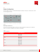
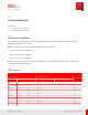
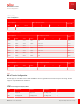
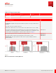
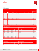
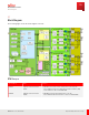
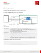
Table Of Contents
- User Guide
- Contents
- Preface
- 1 About this Guide
- 2 Overview
- 3 RU Hardware Feature
- 3.1 System Configuration
- 3.2 RU Specifications
- 3.3 Environment Specifications
- 3.4 RU Downlink/Uplink Default Parameters
- 3.5 Antenna Configuration
- 3.6 Carrier Configuration
- 3.7 Block Diagram
- 3.8 External Interface
- 3.9 TX Control Function
- 3.10 Performance Requirement
- 3.11 Mechanical Design and Other Options
- 4 Ordering Information
- 5 Installation
- 6 Operations
- 7 Maintenance and Trouble Clearing
- 8 Removal
- A References
- B ZTP Overview
- C Optical Connector Cleaning
- D Glossary
- Index

Function Block Name Function
n71n29n26-RF n71n29n26-RF#A n71n29n26-
RF#B
▪ A transmission RF signal from the RF-IC is amplified by a power amplifier
(PA) for each band.
▪ The received RF signal from a DUP is amplified by a low noise amplifier
(LNA).
▪ Transmission digital signal from TRX is converted into a transmission RF
signal after performing D/A conversion and orthogonal modulation at
RF-IC.
Received RF signal from a DUP is demodulated and A/ D converted, and
the received digital signal is outputted to TRX.
DUP Duplexer ▪ The RF signals of each frequency bands (n71, n29, n26) are combined
and separated, and the frequency bands of the transmitted RF signal
and the received RF signal are passed and the out-of-band components
are removed.
PS Power Supply ▪ Provides necessary power supply voltage to the RU from a DC power
supply input (−36.0…−58.0 V DC).
TRX Transmitter and Receiver ▪ It has a high-speed data (baseband signals) interface function of LLB.
It has an interface with the RFIC, to perform DPD and CFR processing of
the transmission signal and Digital Down Conversion (DDC) processing of
the received RF signal.
LLB Lower Layer Baseband ▪ IQ signals in Lower Layer Split (LLS) and monitoring signals are
transmitted between a higher NR system CU device and TRX by an
optical fiber according to an eCPRI format.
RU Hardware Feature
Block Diagram
37
Release 1.0 · Issue 1, March 2021
Fujitsu and Fujitsu Customer Use Only