
User's Guide
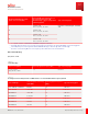
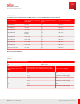
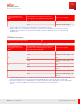
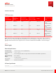
Table Of Contents
- User Guide
- Contents
- Preface
- 1 About this Guide
- 2 Overview
- 3 RU Hardware Feature
- 3.1 System Configuration
- 3.2 RU Specifications
- 3.3 Environment Specification
- 3.4 RU Downlink/Uplink Default Parameters
- 3.5 Antenna Configuration
- 3.6 Carrier Configuration
- 3.7 Block Diagram
- 3.8 External Interface
- 3.9 TX Control Function
- 3.10 Performance Requirement
- 3.11 Mechanical Design and Other Options
- 4 Ordering Information
- 5 Installation
- 6 Operations
- 7 Maintenance and Trouble Clearing
- 8 Removal
- A References
- B ZTP Overview
- C Optical Connector Cleaning
- D Glossary
- Index

In-Channel Selectivity
Table 25
General (SCS=15 kHz)
BS channel
bandwidth (M Hz)
Reference
measurement
channel
W anted signal
mean pow er (dBm)
Interfering signal
mean pow er (dBm)
NF (dB)
Type of interfering
signal
5 G-FR1-A1-7 -100.6 -81.4 NF
REF
+ 3.3 DFT-s-OFDM NR
signal,
15 kHz SCS, 10 RBs
10 G-FR1-A1-1 -98.7 -77.4 NF
REF
+ 3 DFT-s-OFDM NR
signal,
15 kHz SCS, 25 RBs
15 G-FR1-A1-1 -98.7 -77.4 NF
REF
+ 3 DFT-s-OFDM NR
signal,
15 kHz SCS, 25 RBs
20 G-FR1-A1-1 -98.7 -77.4 NF
REF
+ 3 DFT-s-OFDM NR
signal,
15 kHz SCS, 25 RBs
Note: Wanted and interfering signal are placed adjacently around Frequency of the carrier centre frequency
(Fc), where the Fc is defined for BS channel bandwidth of the wanted signal according to the table 5.4.2.2-1. The
aggregated wanted and interferer signal must be centered in the BS channel bandwidth of the wanted signal.
3.10.3
Power Supply
Electrical Specifications
Nominal Voltage Nominal voltage: −48.0 V (ATIS-0600315)
Operating Voltage
Range
−36.0 to −58.0 V
In this voltage, RU satisfies the performance described in this hardware specification.
Abnormal Voltage
Range
0.0 to −36.0 V
Less than −58.0 V
Over Voltage
Transient
−75 V (9.5 ±0.5 ms) (ATIS-0600315)
Criteria: non destruction
DC Power Specification
DC Current 36.5 Amps maximum
RU Hardware Feature
Performance Requirement
60
Release 1.0 · Issue 1, March 2021
Fujitsu and Fujitsu Customer Use Only