
Datasheet


© Copyright 2005-2011 Future Technology Devices International Ltd
9
Document Reference No.: FT_000051
UM232R USB - Serial UART Development Module
Datasheet Version 1.1
Clearance No.: FTDI# 125
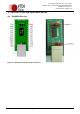
Pin No.
Name
Type
Description
20
RST#
Input
Can be used by an external device to reset the FT232R. If not required can be left
unconnected, or pulled up to VCCIO.
22
CB1
I/O
Configurable CBUS I/O Pin. Function of this pin is configured in the device internal
EEPROM. Factory Default pin Function is RXLED#. See CBUS Signal Options, Table
4.4.*
23
CB0
I/O
Configurable CBUS I/O Pin. Function of this pin is configured in the device internal
EEPROM. Factory Default pin Function is TXLED#. See CBUS Signal Options,Table 4.4.*
Table 4.1Module Pin Out Description
* When used in Suspend, these pins are pulled to VCCIO via internal 200kΩ resistors. These pins
can be programmed to gently pull low during USB suspend (PWREN# = “1”) by setting an option
in the internal EEPROM.
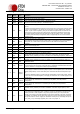
4.3 Jumper Configuration Options
Pin No.
Name
Type
Description
1
3V3
Output
Connect this pin to pin 2 to create 3V3 I/O.
2
VIO
PWR
Input Pin for Chip VCCIO
3
VCC
PWR
Connect this pin to pin 2 to create 5V I/O
Table 4.2 Jumper J1 Pin Description
Pin No.
Name
Type
Description
1
USB
PWR
5V Power output USB port. For a low power USB bus power design, up to 100mA can
be sourced from the 5V supply on the USB bus. A maximum of 500 mA can be sourced
from the USB bus in a high power USB bus powered design.
2
VCC
PWR or
Output
Board supply input. Connect to jumper J2 pin 1 in order to supply the board from the
USB bus.
This pin is internally connected to the VCC DIP pins. Remove the jumper connector in a
self powered design.
Table 4.3 Jumper J2 Pin Description