
Datasheet


6
4.1.4.OUTPUT RISE TIME
(10% TO 90% OF FINAL OUTPUT VALUE, @FULL LOAD)
115V-rms or 230V-rms + 5Vdc : 20ms Maximum
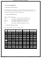
4.1.5.OVER VOLTAGE PROTECTION
+5V
dc
output: +5.7 V
dc minimum, +
6.5V
dc
maximum
+12Vdc output: +13.3Vdc
minimum
,
+
15.6V
dc
maximum
+ 3.3V
dc
output: +3.7Vdc
minimum
,
+
4.5V
dc
maximum
4.1.6.SHORT CIRCUIT PROTECTION
Output short circuit is defined to be a short circuit load of less than 0.1 ohm.
In the event of an output short circuit condition on +3.3V, +5V or +12V output, the power supply
will shutdown and latch off. The power supply shall return to normal operation after the short
circuit has been removed and the power switch has been turned off for no more than 2 seconds.
In the event of an output short circuit condition –12V output, the power supply will not be latch off.
The power supply shall return to normal operation as soon as the short circuit has been removed and
the power switch has been turned off for no more than 2 seconds.
4.1.7.OVERLOAD PROTECTION
Overload currents defined as a 10 amp/sec fault current ramp starting from full load, applied to the
+3.3V, +5V output, shall not cause that output to exceed 35 amps before the output voltage drops
below 0.5 volts and is latched off. The +12V output shall not exceed 25 amps under the same ramp
conditions starting at full load before it is latched off.
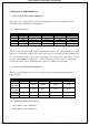
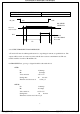
4.1.8.POWER GOOD SIGNAL
The power good signal is a TTL compatible signal for the purpose of initiating an orderly star-up
procedure under normal input operating conditions. This signal is asserted (low) until +5Vdc has
reached 4.75 volts during power up. Characteristics:
TTL signal asserted (low state) : less than 0.5V while sinking 10mA.
TTL signal asserted (high state): greater than 4.75V while sourcing 500uA.
High state output impedance: less or equal to 1Kohm from output to common.
文件資料管制 文件資料管制 文件資料管制
6/11禁止翻印外洩 ESD09081969-R9.pdf 發行時間:2011/6/23 10:56 上午