
Board Users Guide


MPC5200B Users Guide, Rev. 1
20-4 Freescale Semiconductor
Block Diagram
• Low Power Options
The BDLC module can save power in Disabled, Wait, and Stop modes. A complete description of what the BDLC module does
while in a low power mode can be found in Section 20.3, Modes of Operation.
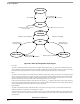
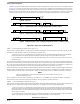
20.4 Block Diagram
Figure 20-2. BDLC Block Diagram
Figure 20-2 shows the organization of the BDLC module. The Buffers provide storage for data received and data to be transmitted onto the
J1850 bus. The Protocol Handler is responsible for the encoding and decoding of data bits and special message symbols during transmission
BCR1
BSVR
BCR2
BDR BARD
CPU INTERFACE
8
8
TX Shadow Register
RX Shadow Register
TX Shift Register
RX Shift Register
Protocol State Machine
To CPU
Control/ Status
TX Data
RX Data
8
TX Data
8
RX Data
Control/ Status
TX Data
RX Data
Symbol Encoder/Decoder
RX Digital
Filter
Loopback
Multiplexer
RX Data
RX Data
RX Data
RXB
TXB
TX Data
To Physical Interface
CPU Interface
Protocol Handler
MUX Interface
bus clock
bus clock
bus clock