
Board Users Guide


SPI Registers—MBAR + 0x0F00
MPC5200B Users Guide, Rev. 1
Freescale Semiconductor 17-5
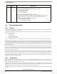
17.3.3 SPI Baud Rate Register—MBAR + 0x0F04
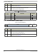
The SPI baud rate is derived from the IPB clock. The SPI module clock divisor is calculated as following:
The SPI Baud rate is calculated as following:
Table 17-7 shows some Baud rates derived from the possible IPB clock values:
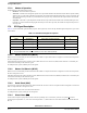
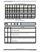
Table 17-5. Bidirectional Pin Configurations
Pin Mode SPC0 MSTR MISO1 MOSI2 SCK3 SS4
A Normal 0 0 Slave Out Slave In SCK in SS
In
B 1 Master In Master Out SCK out SS I/O
C Bidirectional 1 0 Slave I/O GP I/O5 SCK in SS
In
D 1 GP I/O Master I/O SCK out SS
I/O
Note:
1. Slave output is enabled if SPIDDR bit 0 = 1, SS = 0, and MSTR = 0 (A, C).
2. Master output is enabled if SPIDDR bit 1 = 1 and MSTR = 1 (B, D).
3. SCK output is enabled if SPIDDR bit 2 = 1 and MSTR = 1 (B, D).
4. SS
output is enabled if SPIDDR bit 3 = 1, SSOE = 1, and MSTR = 1 (B, D).
5. GP I/O = General-Purpose Input/Output.
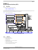
Table 17-6. SPI Baud Rate Register
msb 0 1 2 3 4 5 6 7 lsb
R
Reserved SPPR2 SPPR1 SPPR0 Reserved SPR2 SPR1 SPR0
W
RESET:00000000
Bit Name Description
0—Reserved
1:3 SPPR[0:2] SPI Baud Rate Preselection bits
4—Reserved
5:7 SPR[0:2] SPI Baud Rate Selection bits
SPI module clock divisor SPPR 1+()2
SPR +1()
×=
SPI Baud Rate =
SPI module clock divisor
IPB CLock