
Board Users Guide


MPC5200B Users Guide, Rev. 1
15-44 Freescale Semiconductor
PSC Operation Modes
15.3 PSC Operation Modes
This section describes the different PSC operation modes including the pin muxing, the module configuration, signal definition and some
programming examples. All PSC are independent and can be used at the same time in different modes. But not all PSCs support all modes,
Table 15-73 shows an overview.
In this section the following abbreviations will used as:
15.3.1 PSC in UART Mode
Select the UART mode by writing the corresponding value to the PSC Control (SICR) register. The PSC UART mode is the default mode
after reset. The important registers to configure the PSC for UART mode are:
• SICR register - select the UART mode
• CSR register - select the clock source
• CTUR, CTLR register - select the Baud rate
• MR1 register - select the UART mode (parity mode, bits per character)
• MR2 register - select RTS
and CTS control, Stop Bit Length
• RFALARM, TFALARM - select the FIFO “Alarm” level
• CR register - enable or disable receiver and transmitter
• Port_config - select the right Pin-Muxing, see Chapter 2, Signal Descriptions
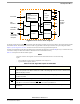
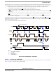
15.3.1.1 Block Diagram and Signal Definition for UART Mode
The Figure 1-1 shows the simplified Block Diagram of the PSC for UART mode.
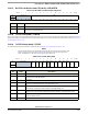
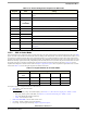
Table 15-73. PSC Modes Overview
PSC1 PSC2 PSC3 PSC4 PSC5 PSC6
UART yes yes yes yes yes yes
Modem / SPI / I2S yes yes yes no no yes
Mclk Generation yes yes yes no no no
AC97 yes yes no no no no
IRDA no no no no no yes
“Cell Phone” master slave slave no no slave
Table 15-74. Clock Short Cuts
Short Cut Description
f
system
Clock from the system PLL
Mclk Clock from the Mclk divider, used as clock input for internal clock generation
or as clock output to an external device. Before modify the counter value the
Mclk divider must be disable. See Section 5.5.11, PSC1 Mclock Config
Register—MBAR + 0x0228 to Section 5.5.14, PSC6 (IrDA) Mclock Config
Register—MBAR + 0x0234.
IP bus Clock Intellectual Property Clock for the internal IP bus system, 33, 66 or 132 MHz,
see Section 5.5, CDM Registers
Mclk =
MclkDiv[8:0] +1
f
system