
Board Users Guide


PSC Registers—MBAR + 0x2000, 0x2200, 0x2400, 0x2600, 0x2800, 0x2C00
MPC5200B Users Guide, Rev. 1
Freescale Semiconductor 15-17
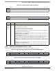
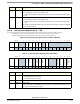
15.2.8 Input Port Change Register (0x10) — IPCR
The read-only IPCR register shows the current state and change-of-state for the Modem control input port.
Table 15-24. Input Port Change Register (0x10) for Codec Mode
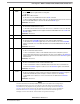
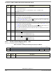
Table 15-22. Tx Buffer Register (0x0c) for Codec24
msb 012345678 9 101112131415
R
Used by Rx Buffer
WTB[0:15]
RESET:0 00000000 0 0 0 00 0 0
16 17 18 19 20 21 22 23 24 25 26 27 28 29 30 31 lsb
R
Used by Rx Buffer
WTB[16:23
Reserved
RESET:0 00000000 0 0 0 00 0 0
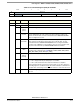
Bit Name Description
0:19
(AC97)
or
0:31
(other)
RB “normal” AC97 (0:19)—Transmit data—AC97 data must be written one complete sample at a
time, where all samples except time slot #0 are 20 bits, time slot #0 data is in bits 0:15. Bit 20 is
1 in the first sample of a new frame.
Bit 20 contains the “Start of Frame Indicator” SOF:
0 = RB[0:19] is not the first sample in the frame.
1 = RB[0:15] is the first sample in a new frame. The number 0 slot is called the TAG slot.
The bits [21:31] are reserved at this mode.
“enhanced” AC97 (0:19)—Transmit data—AC97 data for the expected time slots (3 to 12). The
lower 20 bits contain the valid data word.
UART/SIR/MIR/FIR/Codec8 (0:31)—Transmit data—For these modes, data can be written 1, 2
or 4 bytes at a time. For one byte at a time, all bytes must be written to bits 0:7. For 2 bytes at a
time, data must be written to bits 0:15. Lower-bit data is stored before upper-bit data.
Codec16 (0:31)—Transmit data—For these modes, data can be written 2 or 4 bytes at a time.
For 2 bytes at a time, data must be written to bits 0:15. Lower-bit data is stored before upper-bit
data.
Codec24 (0:23)—Transmit data—For these modes, data must be written 4 bytes at a time. The
lower 24 bits contain the valid data word.
Codec32 (0:31)—Transmit data—For these modes, data must be written 4 bytes at a time.
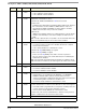
Table 15-23. Input Port Change Register (0x10) for UART/SIR/MIR/FIR Modes
msb 0 1 2 3 4 5 6 7 lsb
R
Reserved D_DCD D_CTS Reserved DCD CTS
W
Reserved
RESET:00000000
msb 0 1 2 3 4 5 6 7 lsb
R SYNC
Reserved D_DCD D_CTS Reserved DCD CTS
W
Reserved
RESET:00000000