
Board Users Guide


ATA Register Interface
MPC5200B Users Guide, Rev. 1
Freescale Semiconductor 11-17
11.3.3.10 ATA Drive Device/Head Register—MBAR + 0x3A78
11.3.3.11 ATA Drive Device Command Register—MBAR + 0x3A7C
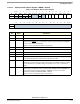
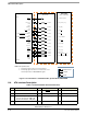
Table 11-28. ATA Drive Device/Head Register
msb 012345678 9 101112131415
R
Rsvd Data Rsvd DEV Data Reserved
W
RESET:0 00000000 0 0 0 00 0 0
16 17 18 19 20 21 22 23 24 25 26 27 28 29 30 31 lsb
R
Reserved
W
RESET:0 00000000 0 0 0 00 0 0
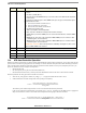
Bits Name Description
0—
Reserved
1 Data Bit is command dependent. In LBA addressing mode, this bit is set to 1 to indicate LBA
addressing is chosen for data transfer.
2—Reserved
3—Reserved
4:7 Data Bit content is command dependent. For most commands, this register indicates the data
transfer starting sector number for when CHS addressing is enabled. This register indicates
part of the LBA address when the LBA addressing is enabled.
This register is written only when ATA drive status register bits BSY and DRQ equal 0 and
DMACK is not asserted. If this register is written when BSY and DRQ bits are set to 1, the
result is indeterminate.
Register content is not valid when drive is in sleep mode.
8:31 — Reserved
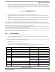
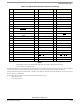
Table 11-29. ATA Drive Device Command Register
msb 0 1 2 3 4 5 6 7 8 9 10 11 12 13 14 15
R
Rsvd HUT FR FE IE UDMA READ WRITE
WData
RESET:0000000000 0000 0 0
16 17 18 19 20 21 22 23 24 25 26 27 28 29 30 31 lsb
R
Reserved
W
RESET:0 000000000 0000 0 0