
Board Users Guide


MPC5200B Users Guide, Rev. 1
9-24 Freescale Semiconductor
Programmer’s Model
9.7.2.2 SCLPC Start Address Register—MBAR + 0x3C04
9.7.2.3 SCLPC Control Register—MBAR + 0x3C08
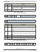
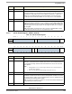
Table 9-14. SCLPC Start Address Register
msb 012345678 9 101112131415
R Start Address
W
RESET:0 00000000 0 0 0 00 0 0
16 17 18 19 20 21 22 23 24 25 26 27 28 29 30 31 lsb
R Start Address
W
RESET:0 00000000 0 0 0 00 0 0
Bits Name Description
0:31 Start Address Address of the first byte in the packet to be sent. This value must be aligned with the
"BPT" (Bytes Per Transaction) field, described below. This address will appear
directly at the peripheral and is completely independent of XLB address decoding
logic.
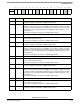
Table 9-15. SCLPC Control Register
msb 012345678 9 101112131415
R
Reserved CSX Reserved Flush RWb
W
RESET:0 00000000 0 0 0 00 0 0
16 17 18 19 20 21 22 23 24 25 26 27 28 29 30 31 lsb
R
Reserved DAI Reserved BPT
W
RESET:0 00000000 0 0 0 00 0 0
Bits Name Description
0:4 — Reserved
5:7 CSX This field should be written with the Chip Select number associated with each DMA
transaction.
Note: LPC configuration registers associated with this CS also affect SCLPC
transactions. The two work together.
8:13 — Reserved
14 Flush If set to 1, enables the assertion of SCLPC requestor at the completion of a *Read*
Packet, regardless of the actual state of the physical fifo ALarm. Requestor will
de-assert once the fifo goes empty. This is the fix for the familiar "Stale Read Data"
fifo problem.
15 RWb Read - Write bar. Controls direction of DMA transaction.
1 = SCLPC will read from the peripheral, i.e. Fifo Receive
0 = SCLPC will write to the peripheral, i.e. Fifo Transmit