
Board Users Guide


MPC5200B Users Guide, Rev. 1
9-18 Freescale Semiconductor
Programmer’s Model
9.7.1.4 Chip Select Status Register—MBAR + 0x031C
9.7.1.5 Chip Select Burst Control Register—MBAR + 0x0328
Bits Name Description
0:6 — Reserved
7 ME Master Enable bit—a global module enable bit. If this bit is low, register access can still occur,
but no external transactions are accepted. However, ME does not affect boot ROM operation
on CS
[0]. If software wishes to disable CS[0], it must write 0 to the Chip Select Boot ROM
Configuration Register enable bit (CE).
8:31 — Reserved
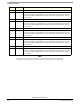
Table 9-10. Chip Select Status Register
msb 012345678 9 101112131415
R
Reserved
WOerr
ROerr
Rsvd CSxerr Reserved
W
RESET:0 00000000 0 0 0 00 0 0
16 17 18 19 20 21 22 23 24 25 26 27 28 29 30 31 lsb
R
Reserved
W
RESET:0 00000000 0 0 0 00 0 0
Bits Name Description
0:1 — Reserved
2 WOerr Write Only error—If 1, it indicates a Read access was attempted on a peripheral marked as
write-only.
This is a sticky bit and must be written with 1 to be cleared. This status bit is always active
regardless of bus error enable bit. The CS number that relates to the error is reflected in the
CSxerr field.
3 ROerr Read Only error—If 1, it indicates a Write access was attempted on a peripheral marked as
read-only.
This is a sticky bit and must be written with 1 to be cleared. This status bit is always active
regardless of bus error enable bit. The CS number that relates to the error is reflected in the
CS
xerr field.
4—Reserved
5:7 CSxerr Chip Select error—Indicates CS number associated with WOerr or ROerr.
8:31 — Reserved
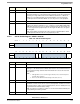
Table 9-11. Chip Select Burst Control Register
msb 0 1 2 3 4 5 6 7 8 9 10 11 12 13 14 15
R CW7 SLB7
Rsvd
BRE7
CW6 SLB6 Rsvd
BRE6
CW5 SLB5 Rsvd
BRE5
CW4 SLB4 Rsvd
BRE4
W
RESET:0000000000000000