
Board Users Guide


MPC5200B Users Guide, Rev. 1
9-2 Freescale Semiconductor
Interface
– (Address 8, 16, 24 or 25 bits, Data 8,16 or 32 bits, 2 Bank Selects)
• 8 Chip Select (CS) signals
— Programmable Wait States per CS
— Programmable Deadcycles per CS
— Programmable Byte Swapping per CS
• Configurable Boot interface supporting PowerPC architecture code execution
• Dynamic bus sizing on some interfaces
• Support of BURST MODE FLASH devices
• DMA (BestComm) support allows data movement independently from the CPU
• NO support of misaligned accesses
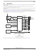
9.3 Interface
The LocalPlus interface consists of:
• Address Bus
•Data Bus
• Chip Select signals CS0-7
• control signals:
—R/W
(Read/Write)
—ALE
(Address Latch Enable)
—ACK
(Acknowledge)
—TS (Transfer Start)
—OE
(Output Enable)
— TSIZ bits (Transfer Size)
— Bank Select bits
• reference clock PCI_CLOCK
The reference clock PCI_CLOCK is always running, even if the PCI Controller is disabled.
9.3.1 External Signals
The external I/O bus is shared with the PCI AD bus and the ATA bus and requires arbitration for access to the external bus.
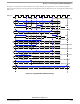
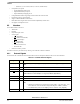
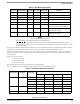
Table 9-1. LocalPlus External Signals
Signal I/O Definition
CS
[7:0] O Chip Selects (active low), CS[4] and CS[5] shared with ATA, CS[6 ] and CS[7] shared with
PSC3.
R/W
O Read/Write. 1 = Read, 0 = Write
EXT_AD[31:0] I/O AD Address / Data bus (bi-directional when used as data; bit 31=msb)
ACK
I/O External Acknowledge input (non-burst transactions),
BURST indication for Most Graphics or Large Flash Modes (Open Drain)
TS
OTransfer Start
OE O Output Enable
TSIZ[1:2] O Transfer Size
Note:
1. TSIZ bits are available in non-muxed modes on GPIO_WKUP_7 and TEST_SEL_1 pins,
if the LPTZ bit is set in the GPS Port Configuration Register—MBAR + 0x0B00
2. The MUXed Mode provides 3 bits TSIZ[0:2], which are available on EX_AD[30:28].
ALE O Address Latch Enable