
Board Users Guide


MPC5200B Users Guide, Rev. 1
8-24 Freescale Semiconductor
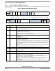
Memory Controller Registers (MBAR+0x0100:0x010C)
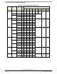
Table 8-8. 32-Bit SDRAM Address Multiplexing
Device Structure
Row bits ×
Col bits ×
Bank bits
hi_
addr
Internal XLA[4:29]
4 5 6 7 8 9:19 20:21 22:29
64Mbit 2Mx32bit 11x8x2 0 —
a
a
All MEM_MA pins are driven in all cases, but only the bits used by memory are listed.
———— RA
[10:0]
BA
[1:0]
CA
[7:0]
4M×16bit 12×8×2 0———— RA[11:0]
8M×8bit 12×9×2 0———CA8
13×8×2 1———RA12
128Mbit 4M×32bit 12×8×2 0———— RA[11:0] BA
[1:0]
CA
[7:0]
8M×16bit 12×9×2 0———CA8
13×8×2 1———RA12
16M×8bit 12×10×20 ——CA9CA8
13×9×21——CA8RA12
256Mbit 8M×32bit 12×9×2 0 — — — CA8 RA[11:0] BA
[1:0]
CA
[7:0]
13×8×2 1———RA12
16M×16bit 12×10×20 ——CA9CA8
13×9×21——CA8RA12
32M×8bit 12×11×2 0 — CA11 CA9 CA8
13×10×2 1 — CA9 CA8 RA12
512Mbit 16M×32bit 12×10×2 0 — — CA9 CA8 RA[11:0] BA
[1:0]
CA
[7:0]
13×9×21——CA8RA12
32M×16bit 12×11×2 0 — CA11 CA9 CA8
13×10×2 1 — CA9 CA8 RA12
64M×8bit 12×12×2 0 CA12 CA11 CA9 CA8
13×11×2 1 CA11 CA9 CA8 RA12
1Gbit 32Mx32bit 12×11×2 0 — CA11 CA9 CA8 RA[11:0] BA
[1:0]
CA
[7:0]
13×10×2 1 — CA9 CA8 RA12
64Mx16bit 12×12×2 0 CA12 CA11 CA9 CA8
13×11×2 1 CA11 CA9 CA8 RA12
2Gbit 64Mx32bit 12×12×2 0 CA12 CA11 CA9 CA8 RA[11:0] BA
[1:0]
CA
[7:0]
13×11×2 1 CA11 CA9 CA8 RA12