
Board Users Guide


Memory Controller Registers (MBAR+0x0100:0x010C)
MPC5200B Users Guide, Rev. 1
Freescale Semiconductor 8-21
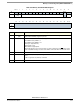
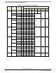
Table 8-5. Memory Controller Mode Register
msb 0123456789101112131415
R
Rsvd
W MEM_MBA
[1:0]
MEM_MA[11:0] cmd
RESET:00000000000000 0 0
16 17 18 19 20 21 22 23 24 25 26 27 28 29 30 31 lsb
R
Reserved
W
RESET:00000000000000 0 0
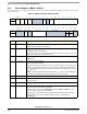
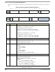
Bit Name Description
0:1 MEM_MBA
[1:0]
See SDRAM data sheet. Select either the memory device Mode register or the memory
device Extended Mode register, if present.
2:13 MEM_MA[11:0] See SDRAM data sheet. MPC5200B supports:
Read CAS Latency, SDR: 2, 3
Read CAS Latency, DDR: 2, 2.5
Burst type: Sequential only
Burst length: 8 only
Other fields: As appropriate
Specific bit allocation can vary from device to device. All devices in all CS spaces must
have compatible format(s), because all are written at the same time with the same value.
14 — Reserved
15 cmd 1 Generate a (Extended) Mode Register Set memory command. Applied to all CS
at
once.
0 Do not generate any memory command.
16:31 — Reserved