
Board Users Guide


General Purpose I/O (GPIO)
MPC5200B Users Guide, Rev. 1
Freescale Semiconductor 7-27
Full Ethernet consumes all 18 pins, unless the optional MDIO and MDC pins are specified as unused. In this case, 2 Output Only GPIO are
available.
Meanwhile, there are other cases becasue many pins can be used for UART, J1850. Please Refer to the port-mapping illustrations for details.
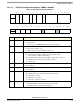
USB stand-alone usage leaves available:
• 2 Output Only GPIO
• 4 Simple GPIO
• 1 WakeUp GPIO
7-wire Ethernet stand-alone leaves available:
• 6 Output Only GPIO
• 4 Interrupt GPIO
• 1 WakeUp GPIO
1850 stand-alone leaves available:
• 7 Output Only GPIO
• 4 Simple GPIO
• 3 Interrupt GPIO
• 1 WakeUp GPIO
Total GPIO available on this port is:
• 8 Output Only GPIO
• 4 Simple GPIO
• 4 Interrupt GPIO
• 1 WakeUp GPIO
7.3.1.6 PSC6
The PSC6 port has 4 pins, which includes:
• 2 Simple GPIO
• 2 WakeUp GPIO
Hardware functions available are:
• IRDA
— 3 pins with clock input
— 2 pins with internal clock
• UART (4 pins)
• Codec (4 pins)
The IRDA clock pin can be used as a Input USB clock and is separately programmable for this use.
• If unused, the IRDA Receive pins are available as WakeUp GPIO.
• If unused, the IRDA Transmit pin and the Clock pin are available as Simple GPIO.
7.3.1.7 I
2
C
There are 2 I
2
C ports consisting of 2 pins each. Although no GPIO is available on these pins, they can be alternately programmed as CAN1
pins (on I
2
C1) and/or as the ATA Chip Selects (on I
2
C2). If the alternate function is specified, the associated I
2
C port is consumed and
unavailable.
7.3.1.8 GPIO Timer Pins
The GPIO Timer port consists of 8 pins. Each pin is driven by a internal timer module, which can do either of the following:
• drive the pin in Output Compare mode and Pulse Width Modulation mode, or
• monitor the pin as input in Input Capture mode.
Additionally, the timer module can operate the pin as a Simple GPIO. This GPIO control is handled in the Timer Module register, see
Section 7.4.4, GPT Registers—MBAR + 0x0600. If the pin is controlled as a GPIO, then the Timer Module timer can be used as an internal
CPU timer.
The Timer pins can be reconfigured for alternate functionality in the Port Configuration Register, as follows:
• Timer pins 0 and 1 can operate as CAN2 Tx/Rx or ATA Chip Selects.
• Timer pins 2–5 can operate as the SPI port.