
Board Users Guide

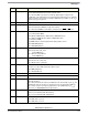


CDM Registers
MPC5200B Users Guide, Rev. 1
Freescale Semiconductor 5-15
NOTE
The clock ratio should only be changed if no module, which is clocked by the IPB and/or PCI clock,
is currently running. Suggestion is to change the clock ratio during the boot time only.
5.5.5 CDM 48MHz Fractional Divider Configuration Register—MBAR + 0x0210
The CDM 48MHz Fractional Divider Configuration Register contains the control bits used in the 48MHz fractional divider.
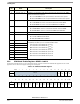
Bit Name Description
0–6 — Reserved for future use. Write 0.
7 ddr_mode SDRAM Controller DDR memory mode, read-only.
bit=0:SDRAM Controller configured for SDR SDRAM (single data rate)
bit=1:SDRAM Controller configured for DDR SDRAM (double data rate)
This register location is a read-only status bit; write 0. The controlling register is in the
SDRAM Controller register map. In the CDM this bit determines the frequency and phase
of memory read clock.
8–14 —
Reserved for future use. Write 0.
15 xlb_clk_sel XLB Clock Frequency
bit=0:XLB CLK = f
system
/4
bit=1:XLB CLK = f
system
/8
This register location is a read-only status bit. The controlling register is the POR
Configuration register - cdm configuration register [26].
16–22 — Reserved for future use. Write 0.
23 ipb_clk_sel IPB Clock Select
bit=0:IPB CLK = XLB_CLK
bit=1:IPB CLK = XLB_CLK/2
24–29 — Reserved for future use. Write 0.
30-31 pci_clk_sel PCI Clock Select
00–PCI_CLK = IPB_CLK
01–PCI_CLK = IPB_CLK/2
10–PCI_CLK = XLB_CLK/4
See also Ta b le 5 -3 and Tabl e 5- 4 .
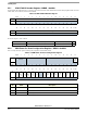
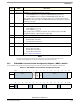
Table 5-12. CDM 48MHz Fractional Divider Configuration Register
msb 0123456789101112131415
R
Reserved
Write 0
ext_usb_
sync_en
ext_usb_
48mhz_en
ext_irda_
48mhz_en
Reserved
Write 0
fd_en
W
RESET: 0 0 0 0000000000000
16 17 18 19 20 21 22 23 24 25 26 27 28 29 30 31 lsb
R
Rsrvd
Write 0
cfgd_p3_cnt
Rsrvd
Write 0
cfgd_p2_cntt
Rsrvd
Write 0
cfgd_p1_cnt
Rsrvd
Write 0
cfgd_p0_cnt
W
RESET: 0 0 0 0000000000000