
Board Users Guide


MPC5200B Users Guide, Rev. 1
4-4 Freescale Semiconductor
Reset Configuration
4.6 Reset Configuration
The MPC5200B is initialized by sampling values found on specific device pins during power-on reset (PORRESET) or hard-reset (HRESET).
These pins are outputs in normal operation, but are sampled as inputs during power-on reset or hard-reset. External pull-up or pull-down
resistors on the board are used to force a value on these pins during power-on reset or hard-reset. These values are latched into the CDM Reset
Configuration register at the end of power-on reset or hard-reset, then distributed to various peripherals. After power-on reset or hard-reset,
these outputs overdrive the external pull-up or pull-down resistors and behave as functional outputs. Only during power-on reset or hard-reset
these pins are inputs.
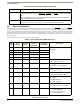
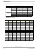
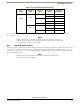
Table 4-2 gives the power-on reset or hard-reset configuration inputs.
JTAG_TRST JTAG reset input. Generated externally from JTAG or debug control logic. This input only resets
the JTAG logic. Other system resets (PORRESET
, HRESET, and SRESET) do not reset the JTAG
logic.
Note: For information on the reset signal JTAG_TRST and the relationship to other reset signals
refer to the MPC5200 Hardware Specifications.
ATA Reset This is NOT a reset pin on MPC5200B. The ATA reset for the external drive must be supplied by
the board level reset source, or if software control is required, generated via a GPIO.
Table 4-2. Reset Configuration Word Source Pins
Pkg
Ball
Reset
Config Pin
I/O Signal
Name
CDM Reset
Config
Register Bit
Config Signal
from CDM
Description
Y18 RST_CFG0 ATA_DACK PORCFG[31] ppc_pll_cfg_4 MPC5200B G2_LE PPC Core PLL
Configuration
Y17 RST_CFG1 ATA_IOR PORCFG[30] ppc_pll_cfg_3
W17 RST_CFG2 ATA_IOW PORCFG[29] ppc_pll_cfg_2
W16 RST_CFG3 LP_RWB PORCFG[28] ppc_pll_cfg_1
V14 RST_CFG4 LP_ALE PORCFG[27] ppc_pll_cfg_0
Y13 RST_CFG5 LP_TS PORCFG[26] xlb_clk_sel bit=0:XLB_CLK=f
system
/ 4
bit=1:XLB_CLK=f
system
/ 8
H02 RST_CFG6 USB1_1 PORCFG[25] sys_pll_cfg_0 bit=0:f
system
=16 x SYS_XTAL_IN
bit=1:f
system
=12 x SYS_XTAL_IN
H03 RST_CFG7 USB1_2 PORCFG[24] sys_pll_cfg1 bit=0:f
vcosys
= f
system
bit=1:f
vcosys
= 2 x f
system
K01 RST_CFG8 ETH0 PORCFG[23] boot_rom_mg bit=0:No Boot in Most Graphics Mode
1
bit=1:Boot in Most Graphics Mode
1,2,4
K03 RST_CFG10 ETH2 PORCFG[21] ppc_msrip Microprocessor Boot Address/Exception
table location.
bit=0:0000_0100 (hex)
bit=1:FFF0_0100 (hex)
J01 RST_CFG11 ETH3 PORCFG[20] boot_rom_wait bit=0:4 PCI bus clocks of wait state
bit=1:48 PCI bus clocks of wait state
J02 RST_CFG12 ETH4 PORCFG[19] boot_rom_swap bit=0:no byte lane swap, same
endian ROM image
bit=1:byte lane swap, different
endian ROM image
Table 4-1. Module Specific Reset Signals (continued)
Definition