
Circuit Board Reference Manual


Memory Map/Register Definition
MCF548x Reference Manual, Rev. 3
Freescale Semiconductor 26-3
26.2.4 PSCnTXD
PSCnTXD are the transmitter serial data outputs for the PSC modules. The output is held high (mark
condition) when the transmitter is disabled, idle, or in the local loopback mode. The PSCnTXD signals can
be programmed to be driven low (break status) by a command.
Refer to Section 26.3.3.5, “Command Register (PSCCRn),” for information about how to program this
signal function.
26.2.5 Signal Properties in Each Mode
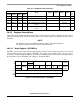
The following table summarizes the signals used for serial communications.
26.3 Memory Map/Register Definition
26.3.1 Overview
This section provides a detailed description of all memory locations and registers. Note that the meaning
of some control register fields depends on the operation mode.
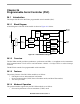
26.3.2 Module Memory Map
The names and address locations of all control registers are listed in Table 26-2.
.
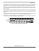
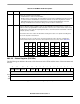
Table 26-1. PSC Signal Properties
Signal Name I/O UART
Modem8
Modem16
AC97 SIR
MIR
FIR
PSCBCLK I — Bit clock — xN bit clock
PSCFSYNC I — Sync — — —
PSCnTXD O Serial transmit data
PSCnRXD I Serial receive data
PSC
nRTS O Transmitter request
to send or Receiver
ready to receive
— Frame sample
sync (48 kHz)
——
PSC
nCTS I Transmitter clear to
send
————
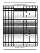
Table 26-2. PSC Memory Map
MBAR Offset
Name Byte0 Byte1 Byte2 Byte3
Access
PSC0 PSC1 PSC2 PSC3
0x8600 0x8700 0x8800 0x8900 PSC Mode register 1, 2
PSCMR1,
PSCMR2
—
R/W
0x8604 0x8704 0x8804 0x8904 PSC Status Register
PSCSR —
R
PSC Clock Select Register
PSCCSR —
W
0x8608 0x8708 0x8808 0x8908 PSC Command Register
PSCCR –
W