
Circuit Board Reference Manual


Application Information
MCF548x Reference Manual, Rev. 3
Freescale Semiconductor 19-71
read and write requests from an XL bus master and decodes them to different address ranges resulting in
the generation of memory, I/O, configuration, interrupt acknowledge and special cycles on the PCI bus.
The window registers are defined in Section 19.3.2.6, “Initiator Window 1 Base/Translation Address
Register (PCIIW1BTAR),” through Section 19.3.2.8, “Initiator Window Configuration Register
(PCIIWCR).”
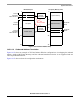
19.5.2 Address Maps
The address mapping in MCF548x system is setup by software through a number of base address registers.
. The internal CPU writes the base address value to module base address register MBAR. MBAR holds the
base address for the 256-Kbyte space allocated to internal registers.
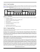
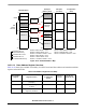
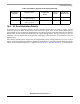
Table 19-57. Transaction Mapping: XL Bus → PCI
XL Bus Transaction
(XL Bus Slave Interface)
Cache Line
Size
Register= 8
Initiator Register Settings
PCI Transaction
Controller
(XL Bus Initiator
Interface) → PCI Target
Initiator Window
Configuration bits
Configuration
Address
Register
IO/M# PRC En
Device
number ==
b1_1111
Single-Beat 1 → 8 byte Read x 0 b00 x x Memory Read
Burst Read (32 bytes) x 0 b00 x x Memory Read
Single-Beat 1 → 8 byte Read x 0 b01 x x Memory Read
Burst Read false 0 b01 x x Memory Read
Burst Read true 0 b01 x x Memory Read Line
Single-Beat 1 → 8 byte Read x 0 b10 x x Memory Read Multiple
Burst Read x 0 b10 x x Memory Read Multiple
Single-Beat 1 → 8 byte, or Burst
Write
x 0 x x x Memory Write
Single-Beat 1 → 4 byte Read x 1 x 0 x I/O Read
Single-Beat 1 → 4 byte Write x 1 x 0 x I/O Write
Single-Beat 1 → 4 byte Read x 1 x 1 false Configuration Read
Single-Beat 1 → 4 byte Write x 1 x 1 false Configuration Write
Single-Beat 1 → 4 byte Read x 1 x 1 true Interrupt acknowledge
Single-Beat 1 → 4 byte Write x 1 x 1 true Special Cycle
—Dual Address Cycles and Memory Write and Invalidate Commands are not supported
—x means “don’t care”