
Circuit Board Reference Manual

MCF548x Reference Manual, Rev. 3
19-58 Freescale Semiconductor
request to the PCI bus comes in, the data transfer is delayed until all previous writes to the PCI bus are
completed. Only when the write buffer is empty can burst data from the XL bus be posted.
19.4.4.1 Endian Translation
The PCI bus is inherently little endian in its byte ordering. The internal XL bus, however, is big endian.
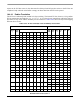
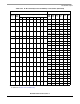
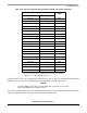
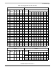
XL bus transactions are limited to 1, 2, 3, 4, 5, 6, 7, 8, or 32 byte (burst) transactions within the data bus
byte lanes on any 32-bit address boundary for burst transfers. Table 19-49 shows the byte lane mapping
between the two buses.
Table 19-49. XL Bus to PCI Byte Lanes for Memory
1
Transactions
XL Bus PCI Bus
A[29:31
]
TSIZ
[0:2]
Data Bus Byte Lanes
AD
[2:0]
BE[3:
0]
31:2
4
23:1
6
15:8 7:0
0123456 7
000 001 OP7 — — — — — — — 000 1110 — — — OP7
001 001 — OP7 — — — — — — 000 1101 — — OP7 —
010 001 — — OP7 — — — — — 000 1011 — OP7 — —
011 001 — — — OP7 — — — — 000 0111 OP7 — — —
100 001 — — — — OP7 — — — 100 1110 — — — OP7
101 001 — — — — — OP7 — — 100 1101 — — OP7 —
110 001 — — — — — — OP7 — 100 1011 — OP7 — —
111 001 — — — — — — — OP7 100 0111 OP7 — — —
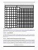
000 010 OP6 OP7 — — — — — — 000 1100 — — OP7 OP6
001 010 — OP6 OP7 — — — — — 000 1001 — OP7 OP6 —
010 010 — — OP6 OP7 — — — — 000 0011 OP7 OP6 — —
011 010 — — — OP6 OP7 — — — 000 0111 OP6 — — —
100 1110 — — — OP7
100 010 — — — — OP6 OP7 — — 100 1100 — — OP7 OP6
101 010 — — — — — OP6 OP7 — 100 1001 — OP7 OP6 —
110 010 — — — — — — OP6 OP7 100 0011 OP7 OP6 — —
000 011 OP5 OP6 OP7 — — — — — 000 1000 — OP7 OP6 OP5
001 011 — OP5 OP6 OP7 — — — — 000 0001 OP7 OP6 OP5 —
010 011 — — OP5 OP6 OP7 — — — 000 0011 OP6 OP5 — —
100 1110 — — — OP7
011 011 — — — OP5 OP6 OP7 — — 000 0111 OP5 — — —
100 1100 — — OP7 OP6
100 011 — — — — OP5 OP6 OP7 — 100 1000 — OP7 OP6 OP5
101 011 — — — — — OP5 OP6 OP7 00 0001 OP7 OP6 OP5 —