
Circuit Board Reference Manual


MCF548x Reference Manual, Rev. 3
18-32 Freescale Semiconductor
18.8.10 Clear the Reset DLL Bit in the Mode Register
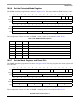
The SDMR should be programmed as shown in Figure 18-20. This step programs the mode register and
enables normal operation of the DLL by clearing the “reset DLL” option.
This configuration results in a value of SDMR = 0x008D_0000, as described in Table 18-21.
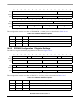
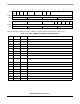
27–26 — 00 Reserved. Should be cleared.
25–24 MUX 01 01 is the MUX setting for a 13 x 9 x 4 memory. See Table 18-2.
23 AP 0 0 sets the auto precharge control bit to A10.
22 DRIVE 0 Data and DQS lines are only driven for a write cycle.
21–16 RCNT 001101 RCNT = (t
REFI
/ (SDCLK x 64)) - 1 = (7800ns/(8.3ns x 64)) - 1 = 13.62, round
down to 13 (0xD)
15–12 — 0000 Reserved. Should be cleared.
11–8 DQS_OE 0000 0x0 disables drive for all SDDQS pins for now.
7–5 — 000 Reserved. Should be cleared.
4 BUFF 0 0 indicates that a buffered memory module is not being used.
3 — 0 Reserved. Should be cleared.
2 IREF 1 Initiate a REF command.
1 IPALL 0 Do not initiate a PALL command.
0 — 0 Reserved. Should be cleared.
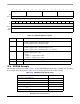
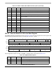
31 30 29 28 27 26 25 24 23 22 21 20 19 18 17 16
Field BNKAD OP_MODE CASL BT BLEN — CMD
Setting 0000_0000_1000_1101
(hex) 0 0 8 D
1514131211109876543210
Field —
Setting 0000_0000_0000_0000
(hex) 0 0 0 0
Figure 18-23. SDRAM Mode/Extended Mode Register Settings
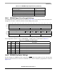
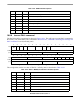
Table 18-24. SDMR Field Descriptions
Bits Name Setting Description
31–30 BNKAD 00 00 selects the mode register.
29–25 OP_MODE 0000 Selects normal operating mode.
24–22 CASL 010 CAS latency of two clocks.
Table 18-23. SDCR + MODE_EN and IREF Field Descriptions (Continued)
Bits Name Setting Description