
Circuit Board Reference Manual


SDRAM Example
MCF548x Reference Manual, Rev. 3
Freescale Semiconductor 18-25
18.8.1 SDRAM Signal Drive Strength Settings
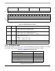
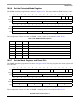
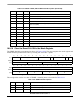
The SDRAMDS should be programmed as shown in Figure 18-14. The settings assume the normal drive
strength for 2.5V drive, 7.6mA, is sufficient for the loading in the system.
This configuration results in a value of SDRAMDS = 0x0000_02AA, as described in Table 18-15.
18.8.2 SDRAM Chip Select Settings
For this example, the SDRAM will be connected to SDCS0 with a base address of 0x0. All other chip
selects are unused and do not need to be initialized. The CS0CFG should be programmed as shown in
Figure 18-15.
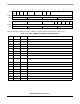
Write recovery timer (t
WR
)15 ns
Precharge command to
ACTV command (t
RP
) 15 ns (min) 18ns (max)
Auto refresh command period (t
RFC
) 72ns (min) 75ns (max)
Average periodic refresh interval (t
REFI
)7.8 µs
31 30 29 28 27 26 25 24 23 22 21 20 19 18 17 16
Field —
Setting 0000_0000_0000_0000
(hex) 0 0 0 0
1514131211109876543210
Field — SB_E SB_C SB_A SB_S SB_D
Setting 0000_0010_1010_1010
(hex) 0 2 A A
Figure 18-14. SDRAM Example Drive Strength Settings (SDRAMDS)
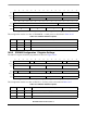
Table 18-15. SDRAMDS Field Descriptions
Bits Name Setting Description
31–10 — 0 Reserved. Should be cleared
9–8 SB_E 10 2.5V, 7.6mA SSTL_2 Class I drive
7–6 SB_C 10 2.5V, 7.6mA SSTL_2 Class I drive
5–4 SB_A 10 2.5V, 7.6mA SSTL_2 Class I drive
3–2 SB_S 10 2.5V, 7.6mA SSTL_2 Class I drive
1–0 SB_D 10 2.5V, 7.6mA SSTL_2 Class I drive
Table 18-14. SDRAM Example Specifications (Continued)
Parameter Specification