
Circuit Board Reference Manual

Memory Map/Register Definition
MCF548x Reference Manual, Rev. 3
Freescale Semiconductor 18-19
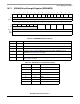
CS3CFG = 94000019 = 64M @ 0x9400 0000-0x97FF FFFF
CS4CFG = 8000001b = 256M @ 0x8000 0000-0x8FFF FFFF
CS5CFG = 00000000 = disable
This gives 400 Mbyte total memory, at 0x8000 0000-0x98FF FFFF
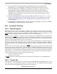
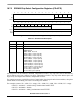
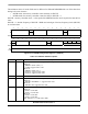
18.7.3 SDRAM Mode/Extended Mode Register (SDMR)
The SDMR, shown in Figure 18-10, is used to write to the mode and extended mode registers that
physically reside within in the SDRAM chips. These registers must be programmed during SDRAM
initialization. See Section 18.5.2, “Power-Up Initialization” for more information on the initialization
sequence.
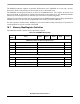
31 30 29 28 27 26 25 24 23 22 21 20 19 18 17 16
R BNKAD AD 0 CMD
W
Reset Uninitialized
1514131211109876543210
R0000000000000000
W
Reset0000000000000000
Reg
Addr
MBAR +0x0100
Figure 18-10. SDRAM Mode/Extended Mode Register (SDMR)
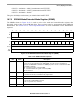
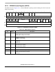
Table 18-10. SDMR Field Descriptions
Bits Name Description
31–30 BNKAD Bank address. Driven onto SDBA[1:0] along with a LMR/LEMR command. All SDRAM chip
selects are asserted simultaneously. SDCR[CKE] must be set before attempting to
generate an LMR/LEMR command. The SDBA[1:0] value is used to select between LMR
and LEMR commands.
00 Load mode register command (LMR)
01 Load extended mode register command (LEMR)
10–11 Reserved
29–18 AD Address. Driven onto SDADDR[11:0] along with an LMR/LEMR command. The AD value
is stored as the mode (or extended mode) register data.
17 — Reserved. Should be cleared.
16 CMD Command.
1 Generate an LMR/LEMR command
0 Do not generate any command
15–0 — Reserved. Should be cleared.