
Circuit Board Reference Manual

MCF548x Reference Manual, Rev. 3
18-8 Freescale Semiconductor
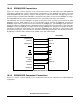
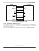
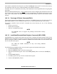
Figure 18-4. MCF548x Connections to 100-pin DDR SDRAM DIMM
18.4.5 DDR SDRAM Layout Considerations
Due to the critical timing for DDR SDRAM, there are a number of considerations that should be taken into
account during PCB layout:
• Minimize overall trace lengths.
• Each DQS, DM, and DQ group must have identical loading and similar routing to maintain timing
integrity.
• Control and clock signals are routed point-to-point.
• Trace length for clock, address, and command signals should match.
• Route DDR signals on layers adjacent to the ground plane.
• Use a VREF plane under the SDRAM.
• VREF is decoupled from both SDVDD and VSS.
• To avoid crosstalk, keep address and command signals separate from data and data strobes.
• Use different resistor packs for command/address and data/data strobes.
• Use single series, single parallel termination (25 Ω series, 50 Ω parallel values are recommended,
but standard resistor packs with similar values can be substituted).
• Series termination should be between the MCF548x and memory, but closest to the processor.
• The parallel termination at end of the signal line (close to the SDRAM).
• 0.1 uF decoupling for every termination resistor pack.
MCF548X
DDR SDRAM
SDADDR[12:0]
SDDATA[31:0]
SDBA[1:0]
SDCS[1:0]
RAS
CAS
SDWE
SDCKE
SDCLK[1:0]
SDCLK
[1:0]
SDDM[3:0]
SDDQS[3:0]
CLK[1:0]
CLK
[1:0]
CKE
S[1:0]
RAS
CAS
WE
DM[3:0]
BA[1:0]
A[12:0]
DQ[31:0]
DQS[3:0]
SCL
SDA
SCL
SDA
SA0
SDVDD