
Circuit Board Reference Manual

MCF548x Reference Manual, Rev. 3
17-24 Freescale Semiconductor
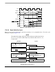
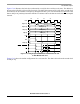
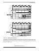
Figure 17-22. Read Bus Cycle with Two Clock Address Setup (No Wait States)
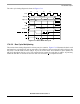
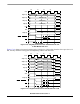
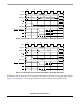
Figure 17-23. Write Bus Cycle with Two Clock Address Setup (No Wait States)
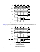
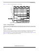
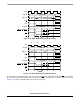
In addition to address setup, there is also a programmable address hold option for each chip select. Address
and attributes can be held one to four clocks after chip select, byte selects, and output enable negate.
Figure 17-24 and Figure 17-25 show read and write bus cycles with two clocks of address hold.
CLK
AD[X:0]
AD[31:Y]
R/W
ALE
TA
OE
S0 AS S1 S2 S3
FBCSn, BE/BWEn
ADDR[X:0]
A[31:Y]
TSIZ[1:0]
TSIZ[1:0]
DATA
CLK
AD[X:0]
AD[31:Y]
R/W
ALE
TA
OE
S0 AS S1 S2 S3
FBCSn, BE/BWEn
ADDR[X:0]
DATA
TSIZ[1:0]
TSIZ[1:0]
A[31:Y]