
Circuit Board Reference Manual

MCF548x Reference Manual, Rev. 3
17-16 Freescale Semiconductor
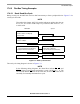
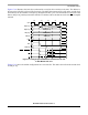
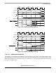
Figure 17-9. Basic Read Bus Cycle
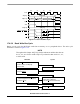
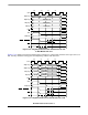
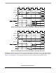
17.6.5.2 Basic Write Bus Cycle
During a write cycle, the MCF548x sends data to memory or to a peripheral device. The write cycle
flowchart is shown in Figure 17-10.
NOTE
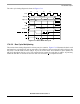
Throughout this chapter AD[X:0] is used to indicate an address bus that can
be 32-, 24-, or 16-bits in width. AD[31:Y] is a data bus that can be 32-, 16-,
or 8-bits wide.
Figure 17-10. Write Cycle Flowchart
CLK
AD[X:0]
AD[31:Y]
R/W
ALE
FBCSn
, BE/BWEn
TA
OE
S0 S1 S2 S3
ADDR[X:0]
A[31:Y] DATA
TSIZ[1:0]
TSIZ[1:0]
1. Select the appropriate slave device.
Drive data on AD[31:Y].
Assert TA
(external termination).
2.
3.
1.
Negate TA (external termination).
1.
Decode address.
1. Set R/W to write.
Place address on AD[31:0].
Assert ALE.
2.
3.
1.
Negate ALE.
Assert FBCS
n.2.
1.
CS unit asserts internal TA (auto
acknowledge/internal termination).
Sample TA
low.2.
1.
Start next cycle.
MCF548X System