
Circuit Board Reference Manual

Memory Map/Register Definition
MCF548x Reference Manual, Rev. 3
Freescale Semiconductor 15-25
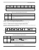
15.3.2.9 PCI Grant Pin Assignment Register (PAR_PCIBG)
The PAR_PCIBG register controls the functions of the PCI grant pins. The PAR_PCIBG register is
read/write.
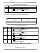
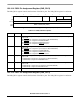
3 PAR_SDA SDA Pin Assignment. Configures the SDA pin for its primary function or general purpose I/O.
0 SDA pin configured for general purpose input (PFECI2C1)
1 SDA pin configured for SDA function
2 PAR_SCL SCL Pin Assignment. Configures the SCL pin for its primary function or general purpose I/O.
0 SCL pin configured for GPIO (PFECI2C0)
1 SCL pin configured for SCL function
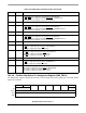
1PAR_
IRQ6
IRQ6
Pin Assignment. Configures the IRQ6 pin for one of its primary functions.
0IRQ6 pin configured for FlexCAN CANRX1
1IRQ6
pin configured for IRQ6 function
Note that GPIO is obtained on the IRQ6 pin by (1) writing a 1 to PAR_IRQ6 and (2) disabling the
IRQ6 function in the EPORT module.
0PAR_
IRQ5
IRQ5 Pin Assignment. Configures the IRQ5 pin for one of its primary functions.
0IRQ5
pin configured for FlexCAN CANRX1
1IRQ5 pin configured for IRQ5 function
Note that GPIO is obtained on the IRQ5 pin by (1) writing a 1 to PAR_IRQ5 and (2) disabling the
IRQ5 function in the EPORT module.
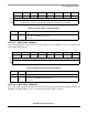
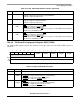
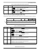
15 14 13 12 11 10 9 8 7 6 5 4 3 2 1 0
R000000 PAR_
PCIBG4
PAR _
PCIBG3
PAR _
PCIBG2
PAR _
PCIBG1
PAR _
PCIBG0
W
Reset0000000000000000
Reg
Addr
MBAR + 0xA48 (PAR_PCIBG)
Figure 15-26. PCI Grant Pin Assignment Register (PAR_PCIBG)
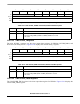
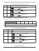
Table 15-28. PAR_PCIBG Field Descriptions
Bits Name Description
15–10 — Reserved, should be cleared.
9–8 PAR_
PCIBG4
PCIBG4
pin assignment. Configures the PCIBG4 pin for one of its primary functions or GPIO.
0X PCIBG4
pin configured for general purpose I/O (PPCIGNT4)
10 PCIBG4 pin configured for FlexBus TBST function
11 PCIBG4
pin configured for PCIBG4 function
7–6 PAR_
PCIBG3
PCIBG3 pin assignment. Configures the PCIBG3 pin for one of its primary functions or GPIO.
0X PCIBG3
pin configured for general purpose I/O (PPCIGNT3)
10 PCIBG3 pin configured for GP timer TOUT3 function
11 PCIBG3
pin configured for PCIBG3 function
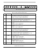
Table 15-27. PAR_FEC/I2C/IRQ Field Descriptions (Continued)
Bits Name Description