
Circuit Board Reference Manual

Memory Map/Register Definition
MCF548x Reference Manual, Rev. 3
Freescale Semiconductor 15-21
15.3.2.5 Port x Pin Assignment Registers (PAR_x)
The PAR_x registers select the signal function that will be driven on the physical pin.
15.3.2.5.1 FlexBus Control Pin Assignment Register (PAR_FBCTL)
The FlexBus control pin assignment (PAR_FBCTL) register controls the function of the FlexBus control
signal pins. The PAR_FBCTL register is read/write.
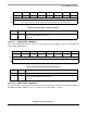
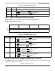
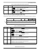
76543210
R00000000
W CLRFB5 CLRFB4 CLRFB3 CLRFB2 CLRFB1
Reset00000000
Reg
Addr
MBAR + 0xA31 (PCLRR_FBCS)
Figure 15-21. 5-Bit FlexBus Clear Output Data Register
Table 15-23. 5-Bit PCLRR_FBCS Field Descriptions
Bits Name Description
7–6 — Reserved, should be cleared
5–1 CLRFBn PCLRR_FBCS clear output data register
0 Corresponding PODR_FBCS bit is cleared
1 No effect
0 — Reserved, should be cleared
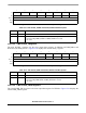
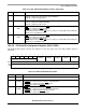
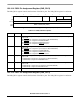
1514131211109876543210
R0 PAR_
BWE3
0PAR_
BWE2
0PAR_
BWE1
0PAR_
BWE0
0PAR_
OE
PAR _RW B 0 PA R_
TA
PAR _A LE
W
Reset0101010101110111
Reg
Addr
MBAR + 0xA40 (PAR_FBCTL)
Figure 15-22. FlexBus Control Pin Assignment Register (PAR_FBCTL)
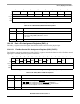
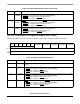
Table 15-24. PAR_FBCTL Field Descriptions
Bits Name Description
15 — Reserved, should be cleared.
14 PAR_BWE3 The PAR_BWE bit configures the BE3/BWE3 pin for its primary function or general purpose I/O.
0 BE3
/BWE3 pin configured for general purpose I/O (PFBCTL7)
1 BE3
/BWE3 pin configured for FlexBus BE3/BWE3 or TSIZ1 function.
The function chosen depends on the reset configuration.
13 — Reserved, should be cleared.