
Circuit Board Reference Manual

MCF548x Reference Manual, Rev. 3
15-18 Freescale Semiconductor
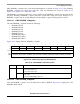
15.3.2.4 Port x Clear Output Data Registers (PCLRR_x)
Writing 0s to a PCLRR_x register clears the corresponding bits in the PODR_x register. Writing 1s has no
effect. Reading the PCLRR_x register returns 0s.
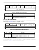
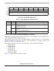
Most PCLRR_x registers have a full 8-bit implementation, as shown in Figure 15-17. The remaining
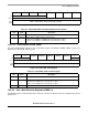
PCLRR_x registers use fewer than eight bits. Their bit definitions are shown in Figure 15-18,
Figure 15-19, Figure 15-20, and Figure 15-21.
The PCLRR_x registers are read/write. The 8-bit PCLRR_x registers include the following:
• PCLRR_FBCTL
• PCLRR_FEC0H
• PCLRR_FEC0L
• PCLRR_FEC1H
• PCLRR_FEC1L
• PCLRR_PSC3PSC2
• PCLRR_PSC1PSC0
Figure 15-17 displays the 8-bit PCLRR_x registers.
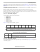
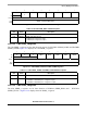
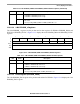
76543210
R 0 0 PPDx5 PPDx4 PPDx3 PPDx2 PPDx1 0
W PSDx5 PSDx4 PSDx3 PSDx2 PSDx1
Reset 0 0 P
1
P
1
P
1
P
1
P
1
0
Reg
Addr
MBAR + 0xA21 (PDDSDR_FBCS)
1
P = the current pin state.
Figure 15-16. 5-Bit PDDSDR_FBCS Register
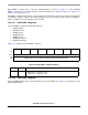
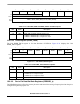
Table 15-18. 5-Bit PDDSDR_FBCS Field Descriptions
Bits Name Description
7–6 — Reserved, should be cleared.
5–1 PPDxn PDDSDR_FBCS pin data. This is Read-only.
0PFBCSn pin state is low
1PFBCSn pin state is high
PSDxn PDDSDR_FBCS set data.
0 No effect
1 Corresponding PODR_FBCS bit is set
0 — Reserved, should be cleared.