
Circuit Board Reference Manual

Register Definition
MCF548x Reference Manual, Rev. 3
Freescale Semiconductor 6-7
6.3 Register Definition
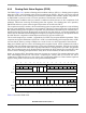
The programmer’s model for the FPU consists of the following:
• Eight 64-bit floating-point data registers (FP0–FP7)
• One 32-bit floating-point control register (FPCR)
• One 32-bit floating-point status register (FPSR)
• One 32-bit floating-point instruction address register (FPIAR)
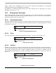
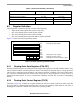
Figure 6-8 shows the FPU programming model.
Figure 6-8. Floating-Point Programmer’s Model
6.3.1 Floating-Point Data Registers (FP0–FP7)
Floating-point data registers are analogous to the integer data registers for the 68K/ColdFire family. They
always contain numbers in double-precision format, even though the operand may be a single-precision
value used in a single-precision calculation. All external operands, regardless of the source data format,
are converted to double-precision format before being used in any calculation or being stored in a
floating-point data register. A reset or a null-restore operation sets FP0–FP7 to positive, nonsignaling
NANs.
6.3.2 Floating-Point Control Register (FPCR)
The FPCR, Figure 6-9, contains an exception enable byte (EE) and a mode control byte (MC). Each EE
bit corresponds to a floating-point exception class. The user can separately enable traps for each class of
floating-point exceptions. The MC bits control FPU operating modes.
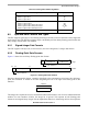
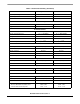
Approximate Ranges
Maximum Positive Normalized 3.4 × 10
38
1.8 x 10
308
Minimum Positive Normalized 1.2 × 10
–38
2.2 x 10
–308
Minimum Positive Denormalized 1.4 × 10
–45
4.9 x 10
–324
63 0
FP0 Floating-point data registers
FP1
FP2
FP3
FP4
FP5
FP6
FP7
FPCR Floating-point control register
FPSR Floating-point status register
FPIAR Floating-point instruction address register
Table 6-3. Real Format Summary (Continued)
Parameter Single-Precision Double-Precision