
Microcontrollers Data Sheet
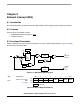


LVI Status and Control Register
MC68HC908MR32 • MC68HC908MR16 Data Sheet, Rev. 6.1
Freescale Semiconductor 99
9.4 LVI Status and Control Register
The LVI status register (LVISCR) flags V
DD
voltages below the V
LVRX
level.
LVIOUT — LVI Output Bit
This read-only flag becomes set when the V
DD
voltage falls below the V
LVRX
voltage for 32 to 40
CGMXCLK cycles. See Table 9-1. Reset clears the LVIOUT bit.
TRPSEL — LVI Trip Select Bit
This bit selects the LVI trip point. Reset clears this bit.
1 = 5 percent tolerance. The trip point and recovery point are determined by V
LVR1
and V
LVH1
,
respectively.
0 = 10 percent tolerance. The trip point and recovery point are determined by V
LVR2
and V
LVH2
,
respectively.
NOTE
If LVIRST and LVIPWR are 0s, note that when changing the tolerance, LVI
reset will be generated if the supply voltage is below the trip point.
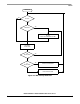
9.5 LVI Interrupts
The LVI module does not generate interrupt requests.
9.6 Wait Mode
The WAIT instruction puts the MCU in low power-consumption standby mode.
With the LVIPWR bit in the configuration register programmed to 1, the LVI module is active after a WAIT
instruction.
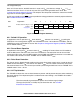
Address: $FE0F
Bit 7654321Bit 0
Read: LVIOUT 0
TRPSEL
00000
Write:RR RRRRR
Reset:00000000
R
=Reserved
Figure 9-3. LVI Status and Control Register (LVISCR)
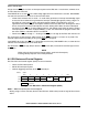
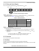
Table 9-1. LVIOUT Bit Indication
V
DD
LVIOUT
At Level: For Number of CGMXCLK Cycles:
V
DD
> V
LVRX
+ V
LVH X
Any 0
V
DD
< V
LVRX
< 32 CGMXCLK cycles 0
V
DD
< V
LVRX
Between 32 & 40 CGMXCLK cycles 0 or 1
V
DD
< V
LVRX
> 40 CGMXCLK cycles 1
V
LVR X
< V
DD
< V
LVRX
+ V
LVH X
Any Previous value