
Microcontrollers Data Sheet


MC68HC908MR32 • MC68HC908MR16 Data Sheet, Rev. 6.1
Freescale Semiconductor 97
Chapter 9
Low-Voltage Inhibit (LVI)
9.1 Introduction
This section describes the low-voltage inhibit (LVI) module, which monitors the voltage on the V
DD
pin
and can force a reset when the V
DD
voltage falls to the LVI trip voltage.
9.2 Features
Features of the LVI module include:
• Programmable LVI reset
• Programmable power consumption
• Digital filtering of V
DD
pin level
• Selectable LVI trip voltage
9.3 Functional Description
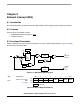
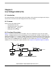
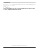
Figure 9-1 shows the structure of the LVI module. The LVI is enabled out of reset. The LVI module
contains a bandgap reference circuit and comparator. The LVI power bit, LVIPWR, enables the LVI to
monitor V
DD
voltage. The LVI reset bit, LVIRST, enables the LVI module to generate a reset when V
DD
falls below a voltage, V
LVRX
, and remains at or below that level for nine or more consecutive CGMXCLK.
V
LVRX
and V
LVHX
are determined by the TRPSEL bit in the LVISCR (see Figure 9-2). LVIPWR and
LVIRST are in the configuration register (CONFIG). See Chapter 5 Configuration Register (CONFIG).
Figure 9-1. LVI Module Block Diagram
LOW V
DD
LVIRST
V
DD
> LVItrip = 0
V
DD
< LVItrip = 1
LVIOUT
LVIPWR
DETECTOR
V
DD
LVI RESET
FROM CONFIG
FROM CONFIG
V
DD
DIGITAL FILTER
CPU CLOCK
ANLGTRIP
TRPSEL
FROM LVISCR