
Microcontrollers Data Sheet

I/O Registers
MC68HC908MR32 • MC68HC908MR16 Data Sheet, Rev. 6.1
Freescale Semiconductor 53
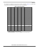
The voltage levels supplied from internal reference nodes as specified in Table 3-1 are used to verify
the operation of the ADC both in production test and for user applications.
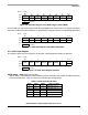
Table 3-1. Mux Channel Select
ADCH4 ADCH3 ADCH2 ADCH1 ADCH0 Input Select
00000 PTB0/ATD0
00001 PTB1/ATD1
00010 PTB2/ATD2
00011 PTB3/ATD3
00100 PTB4/ATD4
00101 PTB5/ATD5
00110 PTB6/ATD6
00111 PTB7/ATD7
01000 PTC0/ATD8
01001
PTC1/ATD9
(1)
1. ATD9 is not available in the 56-pin SDIP package.
01010
Unused
(2)
01011 Ø
01100 Ø
01101 Ø
01110 Ø
01111 Ø
10000 Ø
11010
Unused
(2)
2. Used for factory testing.
11011
Reserved
(3)
3. If any unused channels are selected, the resulting ADC conversion will be unknown.
1
1 1 0 0
Unused
(2)
1 1 1 0 1
V
REFH
1 1 1 1 0
V
REFL
1 1 1 1 1 ADC power off