
Microcontrollers Data Sheet
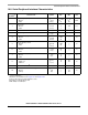

DC Electrical Characteristics
MC68HC908MR32 • MC68HC908MR16 Data Sheet, Rev. 6.1
Freescale Semiconductor 267
19.5 DC Electrical Characteristics
Characteristic
(1)
1. V
DD
= 5.0 Vdc ± 10%, V
SS
= 0 Vdc, T
A
= T
L
to T
H
, unless otherwise noted.
Symbol Min
Typ
(2)
2. Typical values reflect average measurements at midpoint of voltage range, 25°C only.
Max Unit
Output high voltage
(I
Load
= –2.0 mA) all I/O pins
V
OH
V
DD
–0.8
——V
Output low voltage
(I
Load
= 1.6 mA) all I/O pins
V
OL
——0.4V
PWM pin output source current
(V
OH
= V
DD
–0.8 V)
I
OH
–7 — — mA
PWM pin output sink current (V
OL
= 0.8 V) I
OL
20 — — mA
Input high voltage, all ports, IRQ
s, RESET, OSC1
V
IH
0.7 x V
DD
—
V
DD
V
Input low voltage, all ports, IRQ
s, RESET, OSC1
V
IL
V
SS
—
0.3 x V
DD
V
V
DD
supply current
Run
(3)
Wait
(4)
Stop
(5)
3. Run (operating) I
DD
measured using external square wave clock source (f
OSC
= 8.2 MHz). All inputs 0.2 V from rail; no dc
loads; less than 100 pF on all outputs. C
L
= 20 pF on OSC2; all ports configured as inputs; OSC2 capacitance linearly
affects run I
DD
; measured with all modules enabled
4. Wait I
DD
measured using external square wave clock source (f
OSC
= 8.2 MHz); all inputs 0.2 V from rail; no dc loads; less
than 100 pF on all outputs. C
L
= 20 pF on OSC2; all ports configured as inputs; OSC2 capacitance linearly affects wait I
DD
;
measured with PLL and LVI enabled.
5. Stop I
DD
measured with PLL and LVI disengaged, OCS1 grounded, no port pins sourcing current. It is measured through
combination of V
DD
, V
DDAD
, and V
DDA
.
I
DD
—
—
—
—
—
—
30
12
700
mA
mA
µA
I/O ports high-impedance leakage current
I
IL
——±10 µA
Input current (input only pins)
I
In
——±1 µA
Capacitance
Ports (as input or output)
C
Out
C
In
—
—
—
—
12
8
pF
Low-voltage inhibit reset
(6)
6. The low-voltage inhibit reset is software selectable. Refer to Chapter 9 Low-Voltage Inhibit (LVI).
V
LVR 1
4.0 4.35 4.65 V
Low-voltage reset/recover hysteresis
V
LVH 1
40 90 150 mV
Low-voltage inhibit reset recovery
(V
REC1
= V
LVR 1
+ V
LVH 1
)
V
REC1
4.04 4.5 4.75 V
Low-voltage inhibit reset
V
LVR 2
3.85 4.15 4.45 V
Low-voltage reset/recover hysteresis
V
LVH 2
150 210 250 mV
Low-voltage inhibit reset recovery
(V
REC2
= V
LVR 2
+ V
LVH 2
)
V
REC2
4.0 4.4 4.6 V
POR re-arm voltage
(7)
7. Maximum is highest voltage that POR is guaranteed.
V
POR
0—100mV
POR rise time ramp rate
(8)
8. If minimum V
DD
is not reached before the internal POR is released, RST must be driven low externally until minimum V
DD
is reached.
R
POR
0.035 — — V/ms
POR reset voltage
(9)
9. Maximum is highest voltage that POR is possible.
V
PORRST
0 700 800 V
Monitor mode entry voltage (on IRQ
)
V
Hi
V
DD
+ 2.5
—8.0V