
Microcontrollers Data Sheet


MC68HC908MR32 • MC68HC908MR16 Data Sheet, Rev. 6.1
Freescale Semiconductor 101
Chapter 10
Input/Output (I/O) Ports (PORTS)
10.1 Introduction
Thirty-seven bidirectional input-output (I/O) pins and seven input pins form six parallel ports. All I/O pins
are programmable as inputs or outputs.
When using the 56-pin package version:
• Set the data direction register bits in DDRC such that bit 1 is written to a logic 1 (along with any
other output bits on port C).
• Set the data direction register bits in DDRE such that bits 0, 1, and 2 are written to a logic 1 (along
with any other output bits on port E).
• Set the data direction register bits in DDRF such that bits 0, 1, 2, and 3 are written to a logic 1 (along
with any other output bits on port F).
NOTE
Connect any unused I/O pins to an appropriate logic level, either V
DD
or
V
SS
. Although PWM6–PWM1 do not require termination for proper
operation, termination reduces excess current consumption and the
possibility of electrostatic damage.
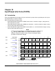
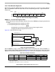
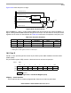
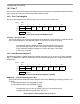
Addr. Register Name Bit 7 6 5 4 3 2 1 Bit 0
$0000
Port A Data Register
(PTA)
See page 103.
Read:
PTA7 PTA6 PTA5 PTA4 PTA3 PTA2 PTA1 PTA0
Write:
Reset: Unaffected by reset
$0001
Port B Data Register
(PTB)
See page 104.
Read:
PTB7 PTB6 PTB5 PTB4 PTB3 PTB2 PTB1 PTB0
Write:
Reset: Unaffected by reset
$0002
Port C Data Register
(PTC)
See page 106.
Read: 0
PTC6 PTC5 PTC4 PTC3 PTC2 PTC1 PTC0
Write: R
Reset: Unaffected by reset
$0003
Port D Data Register
(PTD)
See page 107.
Read: 0 PTD6 PTD5 PTD4 PTD3 PTD2 PTD1 PTD0
Write:RRRRRRRR
Reset: Unaffected by reset
$0004
Data Direction Register A
(DDRA)
See page 103.
Read:
DDRA7 DDRA6 DDRA5 DDRA4 DDRA3 DDRA2 DDRA1 DDRA0
Write:
Reset:00000000
R= Reserved
= Unimplemented
Figure 10-1. I/O Port Register Summary